R8C/1A Group, R8C/1B Group 18. Flash Memory
Rev.1.30 Dec 08, 2006 Page 270 of 315
REJ09B0252-0130
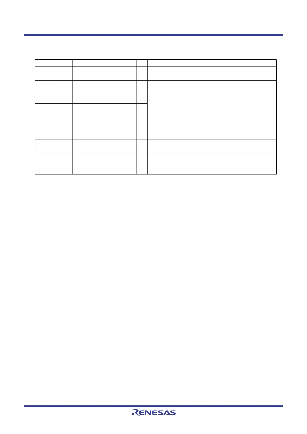
Table 18.8 Pin Functions (Flash Memory Standard Serial I/O Mode 3)
Pin Name I/O Description
VCC,VSS Power input Apply the voltage guaranteed for programming and
erasure to the VCC pin and 0 V to the VSS pin.
RESET
Reset input I Reset input pin.
P4_6/XIN P4_6 input/clock input I Connect a ceramic resonator or crystal oscillator
between pins XIN and XOUT when connecting external
oscillator. Apply “H” and “L” or leave the pin open when
using as input port
P4_7/XOUT P4_7 input/clock output I/O
AVCC, AVSS Analog power supply input I Connect AVSS to VSS and AVCC to VCC,
respectively.
P1_0 to P1_7 Input port P1 I Input “H” or “L” level signal or leave the pin open.
P3_3 to P3_5,
P3_7
Input port P3 I Input “H” or “L” level signal or leave the pin open.
P4_2/VREF,
P4_5
Input port P4 I Input “H” or “L” level signal or leave the pin open.
MODE MODE I/O Serial data I/O pin. Connect to flash programmer.
 Loading...


