R8C/1A Group, R8C/1B Group 19. Electrical Characteristics
Rev.1.30 Dec 08, 2006 Page 294 of 315
REJ09B0252-0130
Timing requirements (Unless Otherwise Specified: VCC = 3 V, VSS = 0 V at Ta = 25 °C) [VCC = 3 V]
Figure 19.13 XIN
Input Timing Diagram when VCC = 3 V
Figure 19.14 CNTR0 Input, CNTR1 Input, INT1
Input Timing Diagram when VCC = 3 V
NOTES:
1. When using the timer C input capture mode, adjust the cycle time to (1/timer C count source frequency x 3) or above.
2. When using the timer C input capture mode, adjust the width to (1/timer C count source frequency x 1.5) or above.
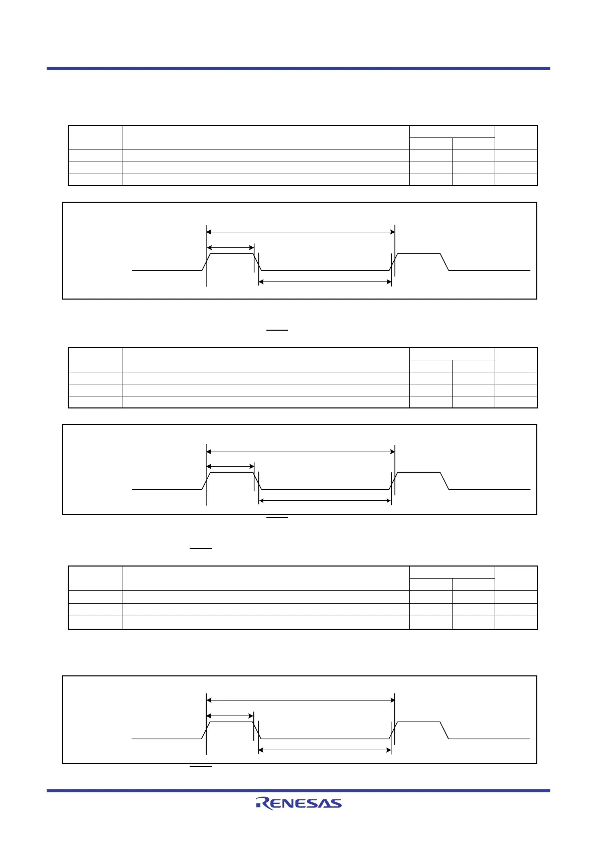
Figure 19.15 TCIN Input, INT3 Input Timing Diagram when VCC = 3 V
Table 19.23 XIN
Input
Symbol Parameter
Standard
Unit
Min. Max.
t
c(XIN) XIN input cycle time 100 − ns
t
WH(XIN) XIN input “H” width 40 − ns
t
WL(XIN) XIN input “L” width 40 − ns
Table 19.24 CNTR0 Input, CNTR1 Input, INT1 Input
Symbol Parameter
Standard
Unit
Min. Max.
t
c(CNTR0) CNTR0 input cycle time 300 − ns
t
WH(CNTR0) CNTR0 input “H” width 120 − ns
t
WL(CNTR0) CNTR0 input “L” width 120 − ns
Table 19.25 TCIN Input, INT3 Input
Symbol Parameter
Standard
Unit
Min. Max.
t
c(TCIN) TCIN input cycle time
1,200
(1)
− ns
t
WH(TCIN) TCIN input “H” width
600
(2)
− ns
t
WL(TCIN) TCIN input “L” width
600
(2)
− ns
XIN input
t
WH(XIN)
tc(XIN)
tWL(XIN)
VCC = 3 V
CNTR0 input
t
WH(CNTR0)
tc(CNTR0)
tWL(CNTR0)
VCC = 3 V
TCIN input
t
WH(TCIN)
tc(TCIN)
tWL(TCIN)
VCC = 3 V
 Loading...


