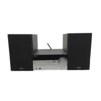
HCD-VM330AV
2727
7-7. NOTE FOR PRINTED WIRING BOARDS AND SCHEMATIC DIAGRAMS
(In addition to this, the necessary note is printed in each block)
C
B
These are omitted.
E
Q
B
These are omitted.
CE
Q
Note on Printed Wiring Boards:
• X : parts extracted from the component side.
• Y : parts extracted from the conductor side.
• W : indicates side identified with part number.
•
f
: internal component.
• : Pattern from the side which enables seeing.
• Indication of transistor.
Note on Schematic Diagram:
• All capacitors are in µF unless otherwise noted. pF: µµF
50 WV or less are not indicated except for electrolytics
and tantalums.
• All resistors are in Ω and
1
/
4
W or less unless otherwise
specified.
•
f
: internal component.
• 2 : nonflammable resistor.
• 5 : fusible resistor.
• C : panel designation.
• A : B+ Line.
• B : B– Line.
• Voltages are taken with a VOM (Input impedance 10 MΩ).
Voltage variations may be noted due to normal produc-
tion tolerances.
• Waveforms are taken with a oscilloscope.
Voltage variations may be noted due to normal produc-
tion tolerances.
• Circled numbers refer to waveforms.
• Signal path.
F : TUNER
J : CD PLAY (ANALOG)
c : CD PLAY (DIGITAL OUT)
g : VIDEO
E : TAPE PLAY (DECK A)
d : TAPE PLAY (DECK B)
G : REC
q : VIDEO IN (AUDIO)
j : GAME IN (AUDIO)
k : GAME IN (VIDEO)
f : 5.1CH INPUT
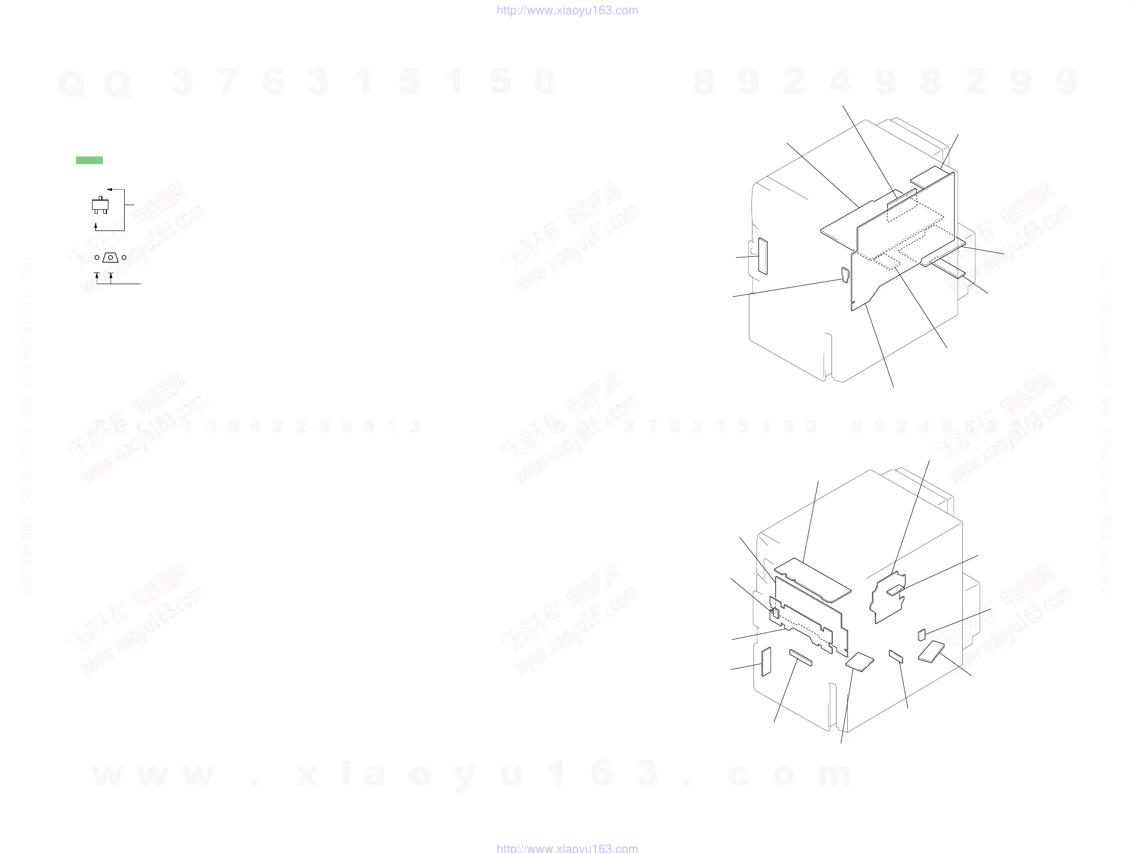
• Circuit Boards Location
CD LED board
GAME LINK board
MAIN AMP board
VIDEO board
FM/AM TUNER PACK
POWER board
VOL SEL board
MAIN board
FUSE board
BD board
D SENSOR (OUT) board
LOAD SW board
L. T MOTOR board
D SENSOR (IN) board
T SENSOR board
DOOR LED board
H/P board
CONTROL board
RMC board
DISPLAY board
TC board
w
w
w
.
x
i
a
o
y
u
1
6
3
.
c
o
m
Q
Q
3
7
6
3
1
5
1
5
0
9
9
2
8
9
4
2
9
8
T
E
L
1
3
9
4
2
2
9
6
5
1
3
9
9
2
8
9
4
2
9
8
0
5
1
5
1
3
6
7
3
Q
Q
TEL 13942296513 QQ 376315150 892498299
TEL 13942296513 QQ 376315150 892498299
http://www.xiaoyu163.com
http://www.xiaoyu163.com
 Loading...