Home
Tektronix
Test Equipment
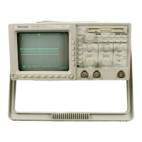
TDS 410A
Tektronix TDS 410A Service Manual
4
of 1
of 1 rating
300 pages
Give review
Manual
Specs
To Next Page
To Next Page
To Previous Page
To Previous Page
Loading...
T
roubleshooting
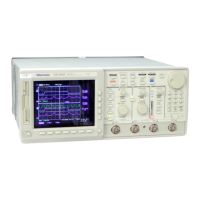
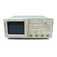
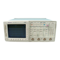
TDS
520A,
524A
,
540A,
&
544A
Service
Manual
6Ć71
J18
pin 1
(Horizontal
Sync)
J18
pin 2
(V
ertical
Sync)
Figure
6Ć35:ăHorizontal
and
Vertical
Sync
Signals
J62
pin 1
(Video)
White
Level
Black
Levels
Blanking
Levels
Figure
6Ć36:ăA
Video
Signal
with
White,
Black,
and
Blanking
Levels
253
255
Table of Contents
Default Chapter
6
Table of Contents
6
Safety Summary
18
Specifications
22
General Product Description
24
User Interface
25
Menus
25
Indicators
25
General Purpose Knob
26
Gui
26
Signal Acquisition System
26
Horizontal System
27
Trigger System
28
Acquisition Control
29
On Board User Assistance
29
Help
29
Autoset
29
Measurement Assistance
29
Cursor
29
Measure
30
Digital Signal Processing (DSP)
30
Storage and I/O
30
Display
31
Zoom
31
Nominal Traits
32
Warranted Characteristics
38
Typical Characteristics
44
Operating Information
48
Using this Manual
50
Before Servicing
50
Strategy for Servicing
50
Manual Structure
51
Manual Conventions
52
Modules
52
Safety
52
Symbols
52
Tektronix Service
53
Warranty Repair Service
53
Repair or Calibration Service
53
Self Service
54
Finding Other Information
54
General Information
56
Supplying Operating Power
56
Power Cord Information
57
Operating Voltage
57
Memory Backup Power
57
Figure 2 1: Power Cord Plug Identification
58
Operating Environment
59
Operating Temperature
59
Ventilation Requirements
59
Applying and Interrupting Power
60
Power on
60
Power off
60
Repackaging Instructions
61
Installed Options
61
General Operating Instructions
62
Screen Layout
62
Basic Procedures
62
How to Power on
62
How to Use Help
63
How to Use the Status Menu
63
Figure 2 2: Map of Display Functions
63
How to Set Functions
64
How to Set Complex Functions
67
Theory of Operation
72
Circuit Description
74
Logic Conventions
74
Module Overview
74
Performance Verification
78
Brief Procedures
80
General Instructions
80
Conventions
81
Figure 4 1: Map of Display Functions
82
Self Tests
83
Verify Internal Adjustment, Self Compensation, and Diagnostics
83
Figure 4 2: Verifying Adjustments and Signal Path Compensation
84
Functional Tests
85
Verify All Input Channels
85
Figure 4 3: Universal Test Hookup for Functional Tests
85
Verify the Time Base
88
Verify the Main and Delayed Trigger Systems
89
Verify the File System (Optional on TDS 520A and 540A)
91
Performance Tests
94
Prerequisites
94
Equipment Required
95
Test Record
98
Signal Acquisition System Checks
102
Check Accuracy of Offset (Zero Setting)
102
Check DC Gain and Voltage Measurement Accuracy
104
Figure 4 4: Measurement of DC Offset Accuracy at Zero Setting
104
Figure 4 5: Initial Test Hookup
105
Figure 4 6: Measurement of the DC Accuracy for Delta
107
Figure 4 7: Measurement of DC Accuracy at Maximum Offset and Position
110
Check Analog Bandwidth
111
Figure 4 8: Initial Test Hookup
111
Figure 4 9: Measurement of Analog Bandwidth
113
Check Delay between Channels
115
Figure 4 10: Initial Test Hookup
115
Figure 4 11: Measurement of Channel Delay
117
Time Base System Checks
118
Check Accuracy for Long Term Sample Rate, Delay Time, and Delta Time Measurements
118
Figure 4 12: Initial Test Hookup
118
Trigger System Checks
121
Check Accuracy (Time) for Pulse Glitch or Pulse Width Triggering
121
Figure 4 14: Initial Test Hookup
121
Figure 4 15: Measurement of Time Accuracy for Pulse and Glitch
123
Check Accuracy, Trigger Level or Threshold, DC Coupled
124
Figure 4 16: Initial Test Hookup
124
Figure 4 17: Measurement of Trigger Level Accuracy
126
Sensitivity, Edge Trigger, DC Coupled
127
Figure 4 18: Initial Test Hookup TDS 520A and 524A Only
128
Figure 4 19: Initial Test Hookup TDS 540A and 544A Only
128
Figure 4 20: Measurement of Trigger Sensitivity
130
Output Signal Checks
133
Check Outputs CH 3 and Main and Delayed Trigger (TDS 540A and 544A Only)
133
Figure 4 21: Initial Test Hookup
133
Figure 4 22: Measurement of Main Trigger out Limits
134
Check Probe Compensator Outputs
136
Figure 4 23: Initial Test Hookup
136
Figure 4 24: Measurement of Probe Compensator Frequency
137
Figure 4 25: Subsequent Test Hookup
138
Figure 4 26: Measurement of Probe Compensator Amplitude
139
Option 05 Video Trigger Checks
140
Check Video Trigger
140
Figure 4 27: Jitter Test Hookup
141
Figure 4 28: Jitter Test Displayed Waveform
141
Figure 4 29: Jitter Test When Completed
143
Figure 4 30: Triggered Signal Range Test - 300
144
Figure 4 31: Triggered Signal Range Test - 75
145
Figure 4 32: 60 Hz Rejection Test Hookup
146
Figure 4 33: 60 Hz Rejection Test Setup Signal
146
Figure 4 34: Subsequent 60 Hz Rejection Test Hookup
147
Figure 4 35: 60 Hz Rejection Test Result
148
Figure 4 36: Line Count Accuracy Test Hookup
149
Figure 4 37: Line Count Accuracy Test Setup Waveform
149
Figure 4 38: Line Count Accuracy Correct Result Waveform
150
Figure 4 39: PG502 Setup for Sync Duty Cycle Test
152
Figure 4 40: Sync Duty Cycle Test: One DIV Neg Pulse Waveform
153
Figure 4 41: Sync Duty Cycle Test: Critically Adjusted Pulse
154
Adjustment Procedures
156
General Information
158
Warm up Period
158
Access
158
Equipment Requirements and Options
159
Computer System and Peripheral Requirements
159
Optional Peripherals
159
Test Equipment
159
Adjustments
159
Performing the Adjustments
159
Complete Adjustment
160
Individual Adjustments
160
Signal Path Compensation
160
Partial Adjustment
160
Adjustment after Repair
161
Adjustment Dependencies
161
Equipment Required
162
Adjustment Instructions
164
Hardware Installation
164
Software Installation
164
Software Based Adjustments
165
Figure 5 1: Accessing the Protection Switch
166
Probe Adjustment
168
Figure 5 2: Hookup for Probe Compensation
168
Compensate the Probe
169
Figure 5 3: Performing Probe Compensation
169
Figure 5 4: Proper and Improper Probe Compensation
169
Measure Probe Bandwidth
170
Figure 5 5: Exposing the Inner Probe Tip
170
Figure 5 6: Initial Test Hookup
171
Adjust the Probe High Frequency Response
172
Figure 5 7: Exposing the Probe Body
173
Figure 5 8: Initial Test Hookup
173
Figure 5 9: Locations of Probe Adjustments
175
Figure 5 10: Adjustments Vs Front Corner Response
175
Display Assembly Adjustment
176
Brightness and Contrast Adjustment (TDS 520A and 540A - Monochrome - Only)
176
Figure 5 11: TDS 520A/540A Five and Ten Percent Luminance
177
Rotation, Brightness, and Contrast Adjustment (TDS 524A and 544A - Color - Only)
179
Figure 5 12: TDS 524A/544A Five and Ten Percent Luminance
180
Maintenance
182
Maintenance Information
184
Procedures Not in this Section
184
Preventing Electrostatic Discharge (ESD)
185
Precautions
185
Susceptibility to ESD
185
Inspection and Cleaning
188
General Care
188
Inspection and Cleaning Procedures
188
Inspection Exterior
189
Cleaning Procedure Exterior
189
Inspection Interior
190
Cleaning Procedure Interior
191
Lubrication
191
Removal and Installation Procedures
192
Preparation Please Read
192
List of Modules
193
General Instructions
193
Summary of Procedures
193
Figure 6 1: External Modules
195
Figure 6 2: Outer Chassis Modules
196
Figure 6 3: Inner Chassis Modules - TDS 520A or 540A with A20 Display Assembly
197
Figure 6 4: Inner Chassis Modules - TDS 524A or 544A with A30 Display Assembly
198
Access Procedure
199
Procedures for External Modules
200
Front Panel Knobs
200
Line Fuse and Line Cord
201
Figure 6 5: Knob Removal
201
EMI Gaskets
202
Figure 6 6: Line Fuse and Line Cord Removal
202
Rear Cover and Cabinet
203
Figure 6 7: Rear Cover and Cabinet Removal
205
Front Cover, Trim Ring, Menu Buttons, and Attenuator Panel
206
Figure 6 8: Front Cover, Trim Ring, Menu Buttons, and Attenuator Panel Removal (Front Cover Not Shown)
206
A12 Front Panel Assembly
208
Figure 6 9: A12 Front Panel Assembly
209
Display Frame Assembly
210
Figure 6 10: Disassembly of Front Panel Assembly
210
Cabinet Modules
212
Figure 6 11: Cabinet Modules Removal
213
Procedures for Outer Chassis Modules
214
A15 Attenuator Assembly
214
Fan
215
Figure 6 12: Attenuator Interconnect Cable Routing and Jack
215
A14 D1 Bus and Power Cables
216
Figure 6 13: A14 D1 Bus and Power Cables Removal
217
A23 Serpar Board: Rs232/Centronics Hardcopy Interface
218
Figure 6 14: Remove Circuit Board Assembly from Oscilloscope
218
Figure 6 15: Remove Circuit Board from Assembly
219
A29 Video Trigger Board
220
Figure 6 16: Circuit Board Installed
221
Figure 6 17: Proper Routing of the Video Cable
222
Figure 6 18: Circuit Board Removal
223
A11 Processor/Display Board
225
Top Cover and Board Brackets
226
Figure 6 19: A11 Processor/Display Removal
226
Figure 6 20: Board Bracket Removal
227
Rear Panel Cables
228
A10 Acquisition Board
228
Figure 6 21: A11 Processor/Display Removal
229
Floppy Disk
230
Figure 6 22: Floppy Disk Removal
231
Rear Chassis
232
Figure 6 23: Rear Chassis Removal
233
Procedures for Inner Chassis Modules
234
A16 Low Voltage Power Supply
234
Figure 6 24: A16 Low Voltage Power Supply Removal
235
A20 or A30 Display Assembly and Supply Fuse
236
Figure 6 25: Display Assembly Removal - TDS 524A and 544A
238
Figure 6 26: Display Assembly Removal - TDS 520A and 540A
239
Figure 6 27: Display Driver Board Removal
240
Front Subpanel
241
Main Chassis
242
Figure 6 28: Front Subpanel Removal
242
Disassembly for Cleaning
243
Troubleshooting
246
TDS 520A, 524A, 540A, & 544A Diagnostics
246
Firmware Updates
247
Figure 6 29: Accessing the Protection Switch
247
Figure 6 30: Primary Troubleshooting Procedure
248
Troubleshooting Procedure
248
Figure 6 31: Module Isolation Troubleshooting Procedure
249
Figure 6 32: A16 Low Voltage Power Supply Module Isolation
250
Figure 6 33: Power Supply Voltage Measurement Locations
252
Figure 6 34: Display Troubleshooting Procedure
253
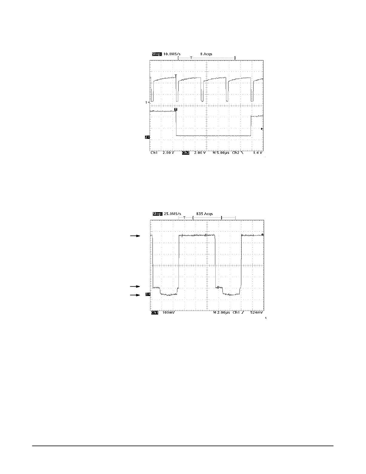
Figure 6 35: Horizontal and Vertical Sync Signals
254
Figure 6 37: Processor/Acquisition Troubleshooting Procedure
255
Figure 6 38: Processor/Front Panel Troubleshooting Procedure
256
Figure 6 39: Attenuator/Acquisition Troubleshooting Procedure
257
Figure 6 40: A11 DRAM Processor/Display Module (View of Right Side)
258
Figure 6 41: A11 DRAM Processor/Display Module (View of Lower Left Corner)
259
Table 7 1: International Power Cords
262
Table 7 2: Standard Accessories
264
Table 7 4: Optional Accessories
265
Table 7 3: Probe Accessories
267
Table 7 5: Probe Accessories
267
Table 7 6: Accessory Software
268
Figure 9 1: Interconnections
277
Figure 9 2: Block Diagram
280
Figure 10 1: Cabinet and Front Panel
288
Figure 10 2: Outer Chassis Modules
290
Figure 10 3: Inner Chassis Modules - A30 Display Shown
292
Figure 10 4: Cables
294
Figure 10 5: Floppy Disk
296
Other manuals for Tektronix TDS 410A
Manual
291 pages
Programming Manual
382 pages
4
Based on 1 rating
Ask a question
Give review
Questions and Answers:
Need help?
Do you have a question about the Tektronix TDS 410A and is the answer not in the manual?
Ask a question
Tektronix TDS 410A Specifications
General
Brand
Tektronix
Model
TDS 410A
Category
Test Equipment
Language
English
Related product manuals
Tektronix TDS 420A
288 pages
Tektronix TDS 220
120 pages
Tektronix TDS 360
65 pages
Tektronix TDS 684A
303 pages
Tektronix TDS 340A
164 pages
Tektronix TDS 500D
376 pages
Tektronix TDS 754D
376 pages
Tektronix TDS 700D
376 pages
Tektronix TDS 520D
376 pages
Tektronix TDS 2012
18 pages
Tektronix TDS 600B
352 pages
Tektronix TDS Series
394 pages
 Loading...