www.ti.com
Clock Source
11
SBAU090E–November 2003–Revised November 2018
Submit Documentation Feedback
Copyright © 2003–2018, Texas Instruments Incorporated
ADS1256EVM and ADS1256EVM-PDK
Table 6. Reference Input Select Switch
Board Marking Switch Position Input Source VRP Connection VRN Connection
EST Down External J1.20 J1.18
OBH Middle Onboard, high common-
mode
AVDD +2.5V
OBL Up Onboard, low common-
mode
+2.5V AGND
In the EXT position, J1 pins 18 and 20 are connected to the ADS1256 reference input.
In the OBH position, the analog power supply is connected to the positive reference input, and the
negative reference input is connected to the output of the onboard reference.
In the OBL position, the onboard reference output is connected to the ADS1256 positive reference input
pin, and the negative reference input pin is grounded.
Both OBH and OBL provide a +2.5V reference to the ADS1256. The OBL position corresponds to the
standard method to connect a reference to the ADS1256, and should be used for most measurements.
The OBH position is useful for testing the reference input common-mode sensitivity, which can be
important for ratiometric connections.
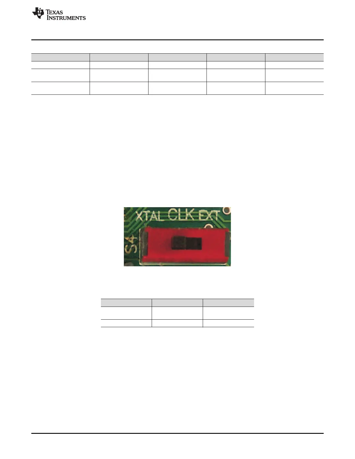
6 Clock Source
As shown in Figure 5, switch S4 selects which of the two available clock sources on the ADS1256EVM
will be provided to the ADS1256. Table 7 summarizes the positions of the switch.
Figure 5. Switch S4
Table 7. System Clock Select Switch
Board Marking Switch Position Clock Source
XTAL Left Onboard 7.68MHz
crystal
EXT Right External (J2 pin 17)

 Loading...