www.ti.com
Using TICS Pro to Program the LMK0482x
15
SNAU145B–MAY 2013–Revised March 2018
Submit Documentation Feedback
Copyright © 2013–2018, Texas Instruments Incorporated
LMK04826 and LMK04828 User’s Guide
5.6 Enable Clock Outputs
While the LMK0482x offers programmable clock output buffer formats, the evaluation board is shipped
with pre-configured output terminations to match the default buffer type for each output.
To measure Phase noise at one of the clock outputs, for example DCLKout0:
1. Click on the Clock Outputs page,
2. Uncheck “CLKoutX_Y_PD” in the Clock Output box to enable the channel,
3. Set the following as needed:
a. Digital Delay value.
b. Clock Divider value (if “Bypass” is not selected as DCLKoutX_MUX).
c. Analog Delay Value (if “Analog Delay and Divider” is selected as DCLKoutX_MUX).
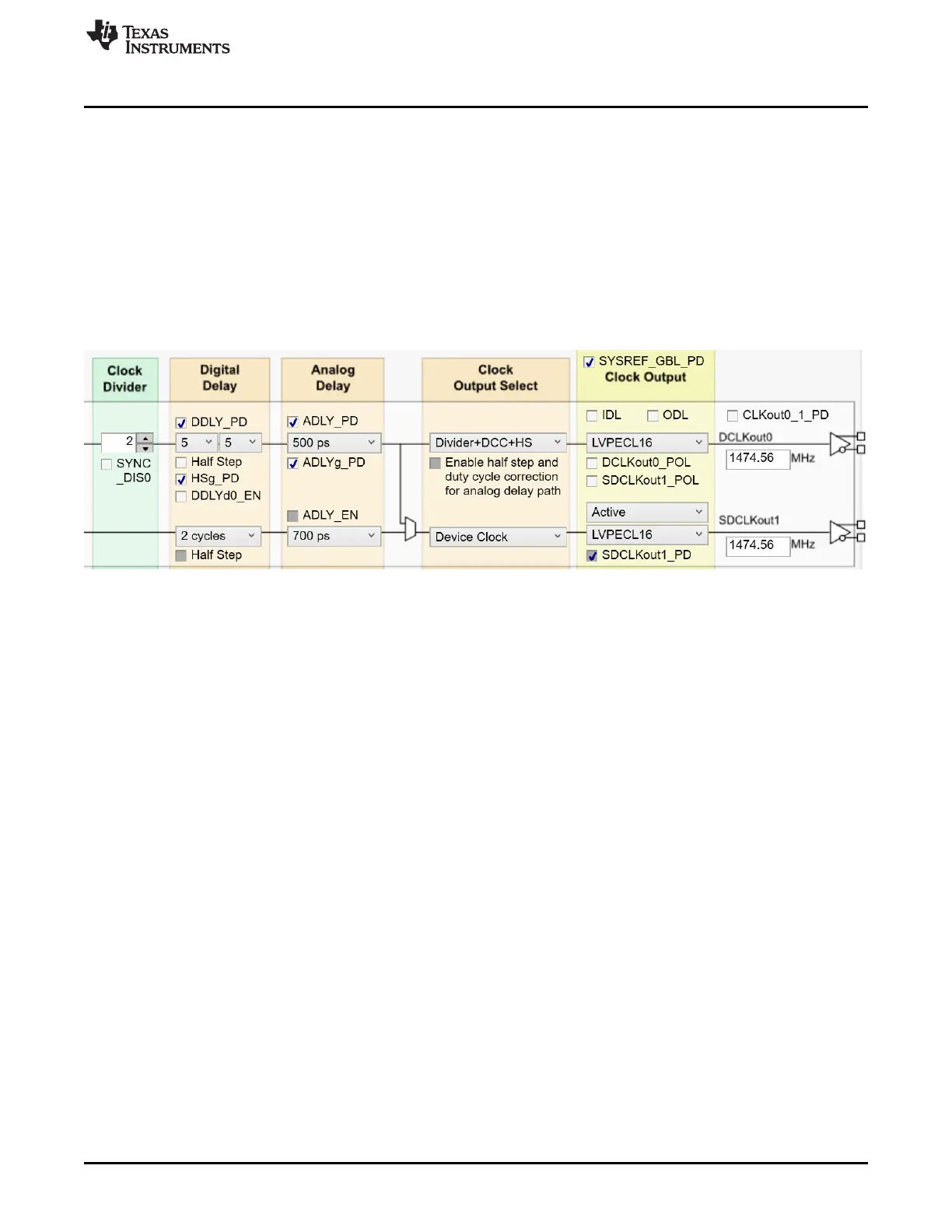
Figure 10. Setting Digital Delay, Clock Divider, Analog Delay and Output Format
4. Depending on the configured output type, the clock output SMAs can be interfaced to a test instrument
with a single-ended 50-Ω input as follows.
a. For LVDS:
i. A balun (like ADT2-1T or high quality Prodyn BIB-100G) is recommended for differential-to-
single-ended conversion.
b. For LVPECL:
I. A balun can be used, or
II. One side of the LVPECL signal can be terminated with a 50-Ω load and the other side can be
run single-ended to the instrument.
c. For HSDS:
I. A balun (like ADT2-1T or high quality Prodyn BIB-100G) is recommended for differential-to-
single-ended conversion.
5. The phase noise may be measured with a spectrum analyzer or signal source analyzer.
TI’s Clock Design Tool can be used to calculate divider values to achieve desired clock output
frequencies. See: http://www.ti.com/tool/clockdesigntool
 Loading...


