1 2 4
22
5 6 7 8 13 14 15 16 17
21
9 11 12
23 24 2625 27 2820
3 10 18 19
Quick Start
www.ti.com
4
SNAU145B–MAY 2013–Revised March 2018
Submit Documentation Feedback
Copyright © 2013–2018, Texas Instruments Incorporated
LMK04826 and LMK04828 User’s Guide
2.1 Quick Start Description
The LMK04828/6 EVM allows full verification of the device functionality and performance specifications.
To quickly set up and operate the board with basic equipment, refer to the quick start procedure below
and test setup shown in Figure 1.
1. Connect a voltage of 4.5 volts to the V
CC
SMA connector or terminal block. Device operates at 3.3 V
using onboard LP3878-ADJ LDO. VCXO operates at 3.3 V using onboard LP5900 LDO.
2. Connect a reference clock to the CLKin1* port from a signal generator or other source. Use 122.88
MHz for default. Exact frequency and input port (CLKin0/CLKin1*) depends on programming.
3. Connect USB2ANY to PC and EVM.
4. Program the device with TICS Pro. TICS Pro is available for download at:
http://www.ti.com/tool/ticspro-sw.
a. Select LMK04828B or LMK04826B from the “Select Device” Menu. Click “Select Device” → “Clock
Generator/ Jitter Cleaner (Dual Loop)” → “LMK0482x”.
b. Select USB2ANY mode from the Communication Setup window. To access this, select “USB
communications” → “Interface”. Confirm PC to USB communications by clicking “Identify” to see
blinking green LED on USB2ANY.
c. Select a default mode from the “Default configuration” Menu. For the quick start use, “CLKin1
122,88 MHz, OSCin 122.88 MHz”.
d. Ctrl+L must be pressed at least once to load all registers. Alternatively click “USB
communications” → “Write All Registers” or the “Write All Registers” button on the Raw Registers
page.
5. Measurements may be made at an active CLKout port through its SMA connector.
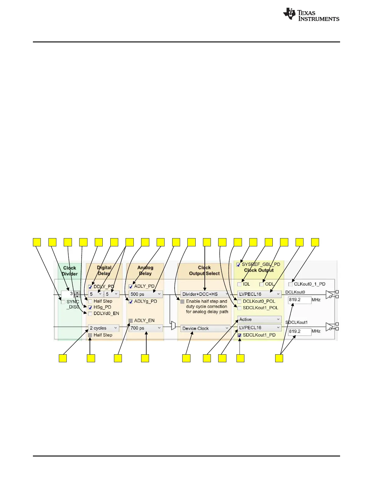
2.1.1 CLKout Page Description
Figure 2. CLKout Page Description Diagram
1. SYNC_DISX: Prevent the divider from being reset by SYNC/SYSREF path.
2. DCLKX_DIV: Divide value for the device clock. If set to 1 then #11 on list must = 1 and #12 must be
Divider+DCC+HS.
3. DDLYdX_EN: Enable dynamic digital delay for this divider.
4. DCLKX_HSg_PD: If clear, glitchless half-step adjustments are enabled.
5. DCLKX_HS: Set half step for this divider. #12 must be Divider+DCC+HS.
6. DCLKX_DDLY_PD: If clear, the digital delay value is assured when a SYNC occurs.
7. DCLKoutX_DDLY_CNTL/CNTH: for controlling the digital delay value.
 Loading...


