29
SNAU145B–MAY 2013–Revised March 2018
Submit Documentation Feedback
Copyright © 2013–2018, Texas Instruments Incorporated
Typical Phase Noise Performance Plots
Appendix B
SNAU145B–MAY 2013–Revised March 2018
Typical Phase Noise Performance Plots
The LMK0482x’s dual PLL architecture achieves ultra low jitter and phase noise by allowing the external
VCXO or Crystal’s phase noise to dominate the final output phase noise at low offset frequencies and the
internal VCO’s phase noise to dominate the final output phase noise at high offset frequencies. This
results in the best overall noise and jitter performance.
Table 6 lists the test conditions used for output clock phase noise measurements with the Crystek 122.88
MHz VCXO.
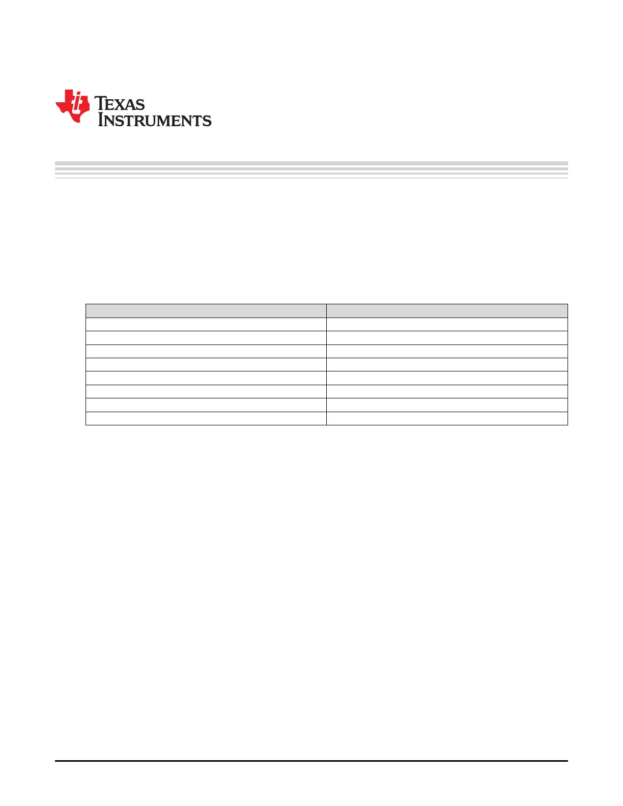
Table 6. LMK0482x Test Conditions
PARAMETER VALUE
PLL1 Reference clock input CLKin1* single-ended input, CLKin1 AC-coupled to GND
PLL1 Reference Clock frequency 122.88 MHz
PLL1 Phase detector frequency 1024 kHz
PLL1 Charge Pump Gain 150 µA
VCXO frequency 122.88 MHz
PLL2 phase detector frequency 122.88 MHz
PLL2 Charge Pump Gain 3200 µA
PLL2 REF2X mode Enabled
 Loading...


