Evaluation Board Inputs and Outputs
www.ti.com
16
SNAU145B–MAY 2013–Revised March 2018
Submit Documentation Feedback
Copyright © 2013–2018, Texas Instruments Incorporated
LMK04826 and LMK04828 User’s Guide
6 Evaluation Board Inputs and Outputs
Table 5 contains descriptions of the inputs and outputs for the evaluation board. Unless otherwise noted,
the connectors described can be assumed to be populated by default. Additionally, some applicable TICS
Pro programming controls are noted for convenience.
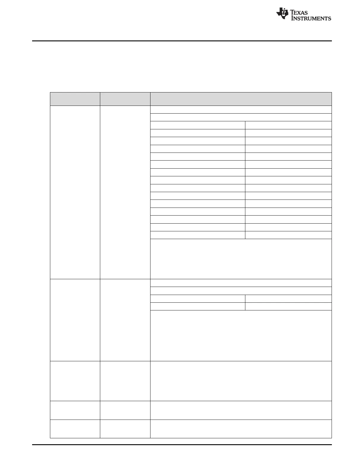
Table 5. Description of Evaluation Board Inputs and Outputs
CONNECTOR NAME
SIGNAL TYPE,
INPUT/OUTPUT
DESCRIPTION
Populated:
DCLKout0,
DCLKout0*,
SDCLKout1,
SDCLKout1*,
DCLKout2,
DCLKout2*,
SDCLKout3,
SDCLKout3*,
DCLKout10,
DCLKout10*
SDCLKout11,
SDCLKout11*
Analog,
Output
Clock outputs with programmable output buffers.
The output terminations by default on the evaluation board are shown below:
Clock Output Pair Default Board Termination
DCLKout0 240 Ω
SDCLKout1 240 Ω
DCLKout2 240Ω
SDCLKout3 240 Ω
DCLKout4 HSDS / LVDS
SDCLKout5 HSDS / LVDS
DCLKout6 HSDS / LVDS
SDCLKout7 HSDS / LVDS
DCLKout8 HSDS / LVDS
SDCLKout9 HSDS / LVDS
DCLKout10 HSDS / LVDS
SDCLKout11 HSDS / LVDS
DCLKout12 HSDS / LVDS
SDCLKout13 HSDS / LVDS
Each CLKout pair has a programmable LVDS, LVPECL, or HSDS buffer. The
output buffer type can be selected in TICS Pro in the Clock Outputs page through
the CLKoutX_TYPE control.
All clock outputs are AC-coupled to allow safe testing with RF test equipment.
All LVPECL clock outputs are terminated using 240 Ω emitter-resistors.
If an output pair is programmed to LVCMOS, each output can be independently
configured (normal, inverted, or off/tri-state).
Populated:
OSCout, OSCout*
Analog,
Output
Buffered outputs of OSCin port.
The output terminations on the evaluation board are shown below.:
OSC Output Pair Default Board Termination
OSCout LVPECL
OSCout has a programmable LVDS, LVPECL, or LVCMOS output buffer. The
OSCout buffer type can be selected in TICS Pro on the Clock Outputs page
through the OSCout_FMT control.
OSCout is AC-coupled to allow safe testing with RF test equipment.
The OSCout output is terminated using 240 Ω emitter-resistors.
If OSCout is programmed as LVCMOS, each output can be independently
configured (normal, inverted, inverted, and off/tri-state).
Best performance/EMI reduction is achieved by using a complementary output
mode like Norm/Inv. It is NOT recommended to use Norm/Norm or Inv/Inv mode.
V
CC
Power,
Input
Main power supply input for the evaluation board.
The LMK0482x contains internal voltage regulators for the VCO, PLL and other
internal blocks. The clock outputs do not have an internal regulator, so a clean
power supply with sufficient output current capability is required for optimal
performance.
On-board LDO regulators and 0 Ω resistor options provide flexibility to supply and
route power to various devices. See the schematics in Appendix C for more details.
Populated:
J1
Power,
Input
Alternative power supply input for the evaluation board using two unshielded wires
(Vcc and GND).
Apply power to either Vcc SMA or J1, but not both.
VccVCXO/Aux
Power,
Input
Optional Vcc input to power the VCXO circuit if separated voltage rails are needed.
The VccVCXO/Aux input can power these circuits directly or supply the on-board
LDO regulators. 0 Ω resistor options provide flexibility to route power.
 Loading...


