ZC706 Evaluation Board User Guide www.xilinx.com 28
UG954 (v1.5) September 10, 2015
Feature Descriptions
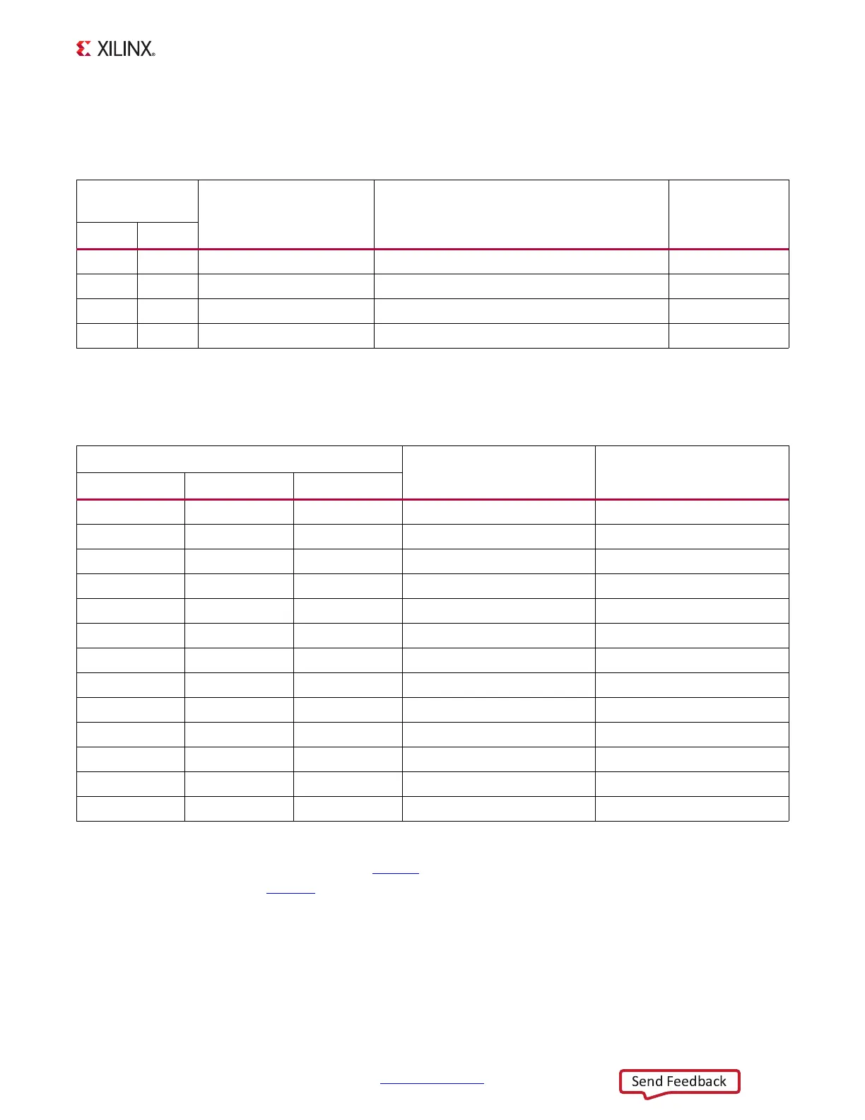
The connections between the USB Micro-B connector at J2 and the PHY at U12 are listed in
Table 1-8.
The connections between the USB 2.0 PHY at U12 and the XC7Z045 AP SoC are listed in
Table 1-9.
For additional information on the Zynq-7000 AP SoC device USB controllers, see Zynq-7000
All Programmable SoC Overview (DS190
) and Zynq-7000 All Programmable SoC Technical
Reference Manual (UG585
).
Table 1-8: USB Connector Pin Assignments and Signal Definitions Between J2 and U12
USB Connector
J1
Net Name Description
USB3320 (U12)
Pin
Pin Name
1 VBUS USB_VBUS_SEL +5V from host system 22
2 D_N USB_D_N Bidirectional differential serial data (N-side) 19
3 D_P USB_D_P Bidirectional differential serial data (P-side) 18
5 GND GND Signal ground 33
Table 1-9: USB 2.0 ULPI Transceiver Connections to the XC7Z045 AP SoC
XC7Z045 (U1)
Schematic Net Name USB3320 (U12) Pin
Pin Name Bank Pin Number
PS_MIO36 501 H17 USB_CLKOUT 1
PS_MIO31 501 H21 USB_NXT 2
PS_MIO32 501 K17 USB_DATA0 3
PS_MIO33 501 G22 USB_DATA1 4
PS_MIO34 501 K18 USB_DATA2 5
PS_MIO35 501 G21 USB_DATA3 6
PS_MIO28 501 L17 USB_DATA4 7
PS_MIO37 501 B21 USB_DATA5 9
PS_MIO38 501 A20 USB_DATA6 10
PS_MIO39 501 F18 USB_DATA7 13
PS_MIO30 501 L18 USB_STP 29
PS_MIO29 501 E8 USB_DIR 31
PS_MIO7 500 D5 USB_RESET_B_AND 27 (via AND gate U13)

 Loading...


