— 11 —
5-2. CIRCUIT EXPLANATION
● FLOW OF PICTURE DATA (Refer to 3. BLOCK DIAGRAM)
1. The picture data from QV camera (digital serial data) are converted into compressed parallel data
(8 bits) by CPU (LSI1), then its data are accumulated in the S-RAM (LSI4).
2. These data are further converted to the corrected color data by CPU (LSI1).
3. Its data are accumulated in the PS-RAM (LSI5, 6) passing through the gate array (LSI2) as the
expanded data.
4. Then, its data are supplied to the thermal head as the printing data passing through the gate array
(LSI2).
● PRINTING METHOD
1. Thermal head prints yellow data using the yellow part of color tape first.
2. Next, thermal head prints reddish violet data using the magenta part of color tape, and then prints
blue data using the cyan part of color tape.
3. Finally, thermal head prints the coating layer using the OP-layer part of the color tape.
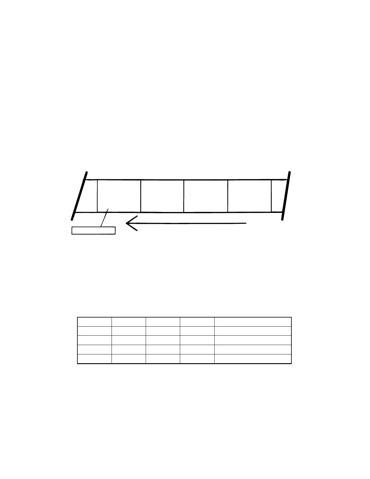
OP-LAYER
COLOR TAPE
YELLOWMAGENTA
CYAN
● LOGIC LEVEL OF SENSOR TERMINAL
Refer to the table on 4. SCHEMATIC DIAGRAMS (4-5. Sensor PCB Z568-2).
● TRUTH TABLE OF DC MOTOR DRIVE IC (BA6885)
Refer to 4. SCHEMATIC DIAGRAMS (4-2. Main PCB Z568-1 (1/2)).
FIN RIN OUT1 OUT2 MODE
H L H L Regular rotation mode
L H L H Reversed rotation mode
H H L L Brake mode
L L OPEN OPEN Stand-by mode
 Loading...