D
24.9 k
(pull-up)
Ω
150 k
Ω
49.9 k
Ω
10 V
A
D
24.9 k
(pull-up)
Ω
150 k
Ω
49.9 k
Ω
10 V
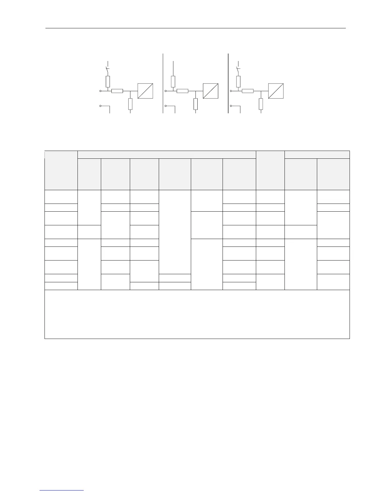
Case 1 Case 2 Case 3
Fig. 21. Input circuit diagram
Table 5. Pull-up resistor handling
pull-up load-free voltage
device
voltage hardware
de-
activated
by @
(8
configured
by DIP
switch
configured
by plug-in
activated
for DI on AI
input
circuit
diagram
(Fig. 21)
with NTC
or low-
impedance
input
for voltage
input or
high-
impedance
input
XF521,
XF521A
fixed NO YES case 2 8.89 V
XF526 fixed NO
NO
YES case 2 8.89 V
XFL521,
XFL521A/B
10 V
YES
(3
config.
(6
case 1
8.89 V
Smart I/O
XFC
5 V
optional
switch-off
YES
(4
YES
YES
(7
case 3 5 V
0 V
XL20 fixed NO YES case 2 8.89 V
XL50
optional
switch-off
YES
(2
YES
(5
case 1 0 V
XL100,
XL100A
fixed
NO
YES case 2 8.89 V
XL100B
NO
YES configurable
XL100C
10 V
optional
switch-off
YES
(1
NO
NO
YES
(5
case 1
8.89 V
0 V
(1
controller firmware ≥ 2.03;
(2
controller firmware ≥ 2.02;
(3
controller firmware ≥ 2.03 (local/shared mode), CARE ≥ 5.00.01 (open mode);
(4
CARE ≥ 5.00.01;
(5
controller firmware < 2.04;
(6
controller firmware < 2.04 (local/shared mode), CARE ≥ 5.01.xx (open mode);
(7
CARE ≥ 5.01.xx;
(8
Assigning "@" as first digit of input characteristic name (e.g.: "@0-10V") in CARE text editor disables the pull-up resistor.
 Loading...