MAINTENANCE
8.7.8 Voltage Source Checks
263 to output lO.OOOOmA to a lk0 resistor. Note that the
voltage checks are referenced to analog common (A). The
Check out the operation of the voltage source by using the
COMMON terminal on the rear panel is analog common.
procedure in Table 8-16. For these checks, program the
Model 263 to output l.OOOOOV.
8.7.8 Digital and Display Circuitry Checks
8.7.7. Electrometer Amplifier Check
Check the various components associated with the digital
and display circuitry using the procedures given in Table
Perform the steps in Table %I7 to check out the electrometer
8-B and 8-19
amplifier circuitry. Set up the AMPS source of the Model
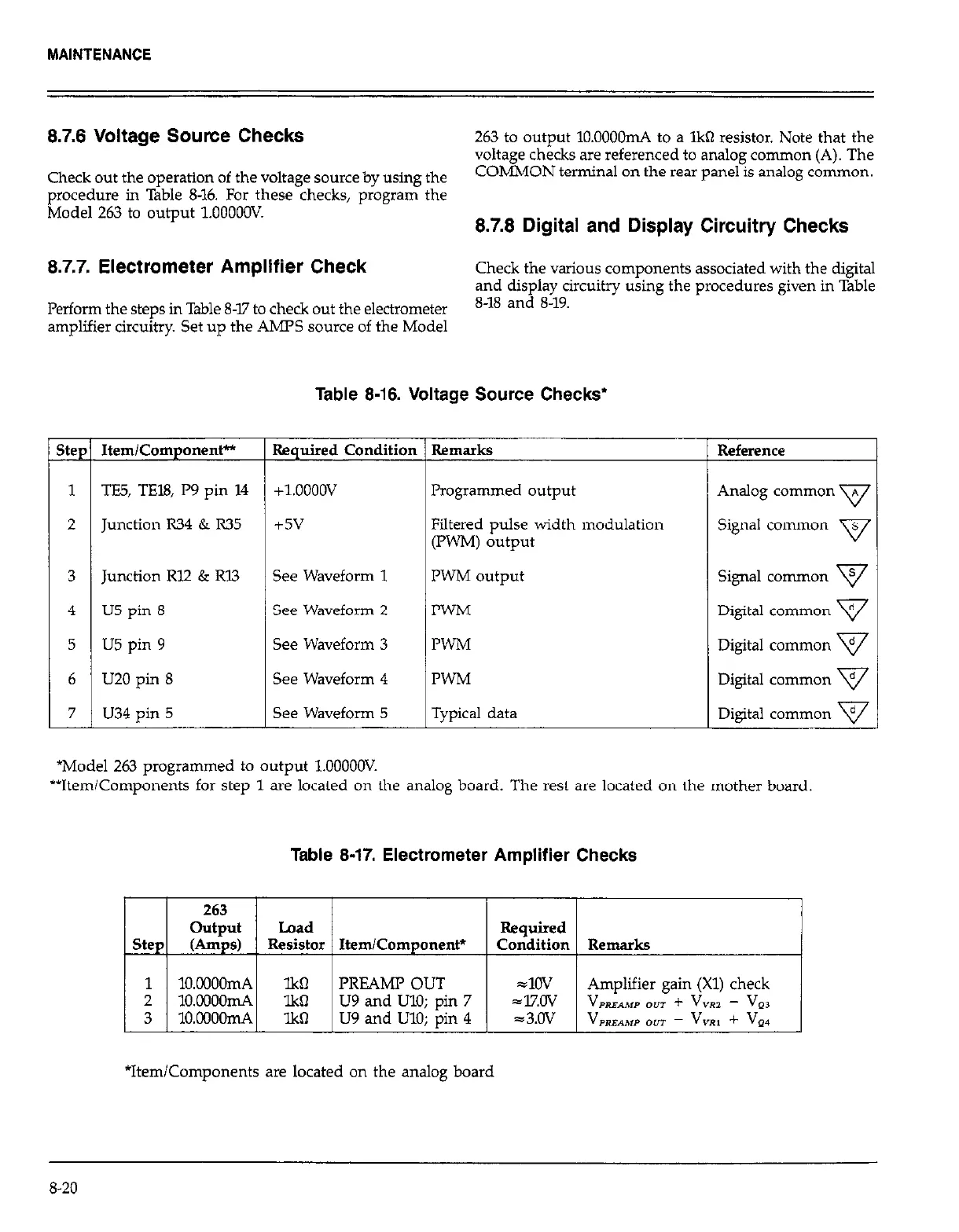
Table 8-16. Voltage Source Checks’
step/ 1temicomponentk
Required Condition
I I
1 TF5, TEl8, P9 pin 14 +1.oooov
2 Junction R34 & R35 +5v
3 Junction Rl2 & Rl3 See Waveform 1
4 U5 pin 8 See Waveform 2
5 IJ5 pin 9 See Waveform 3
6 U20 pin 8 See Waveform 4
7 U34 pin 5 See Waveform 5
Remarks
Programmed output
Filtered pulse width modulation
(PWM) output
I’WM output
PWM
I’WM
PWM
Typical data
Reference
Analog common v
Signal common
v
Signal common
v
Digital common
v
Digital common v
Digital common v
Digital common v
*Model 263 programmed to output l.OOOOOV.
**Item/Components for step 1 are located on the analog board. The rest are located on the mother board.
Table 8-17. Electrometer Amplifier Checks
263
output Load Required
step L4mps) Resistor Item/Component* Condition Remarks
1 1o.oooomA lkQ PRFAMP OUT
=lOV Amplifier gain (Xl) check
1o.oooonL4 lkQ U9 and UlO; pin 7 =l7Jlv
VP.QzAMP OUT + v,, - VLX
1o.cooomA lko U9 and UlO: Din 4 z3.w VP.,,,. nrm - V”.. + vn,
*Item/Components are located on the analog board
S-20
 Loading...