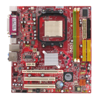
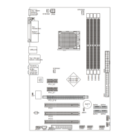
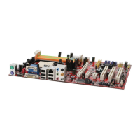
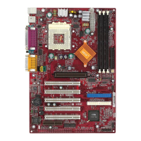
Chapter 3
3-14
Bank Interleave
The field is used to enable or disable memory bank interleave feature.
Settings: Enabled and Disabled.
DRAM Timing by SPD
Selects whether DRAM timing is controlled by the SPD (Serial Presence
Detect) EEPROM on the DRAM module. Setting to Yes enables SDRAM
Advanced Chipset Features
↑↓→←:Move Enter:Select +/-/PU/PD:Value F10:Save ESC:Exit F1:General Help
F5:Previous Values F6:Fail-Safe Defaults F7:Optimized Defaults
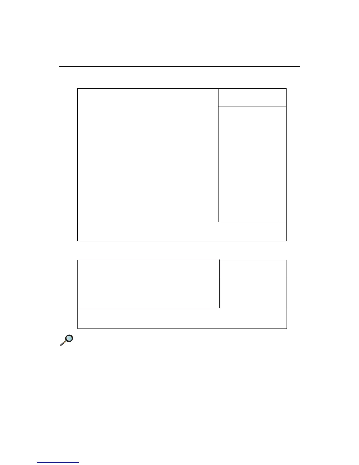
Bank Interleave Enabled
DRAM Timing by SPD Yes
SDRAM CAS Latency Auto
Memory Hole Disabled
P2C/C2P Concurrency Enabled
Fast R-W Turn Around Disabled
System BIOS Cacheable Disabled
Video RAM Cacheable Disabled
AGP Aperture Size 64M
AGP-4X Mode Enabled
AGP Driving Control Auto
AGP Driving Value DA
OnChip USB Enabled
USB Keyboard Support Disabled
USB Mouse Support Disabled
OnChip Sound Auto
OnChip Modem Auto
CPU to PCI Write Buffer Enabled
PCI Dynamic Bursting Enabled
CMOS Setup Utility - Copyright (C) 1984-2000 Award Software
Advanced Chipset Features
Item Help
Menu Level 8
- Next Page -
↑↓→←:Move Enter:Select +/-/PU/PD:Value F10:Save ESC:Exit F1:General Help
F5:Previous Values F6:Fail-Safe Defaults F7:Optimized Defaults
PCI Master 0 WS Write Enabled
PCI Delay Transaction Enabled
PCI#2 Access #1 Retry Disabled
AGP Master 1 WS Write Enabled
AGP Master 1 WS Read Enabled
Memory Parity/ECC Check Disabled
Item Help
Menu Level 8
x
x
Note: Change these settings only if you are familiar with the chipset.
 Loading...