1-4 | ni.com
Chapter 1 NI 651x Fundamentals
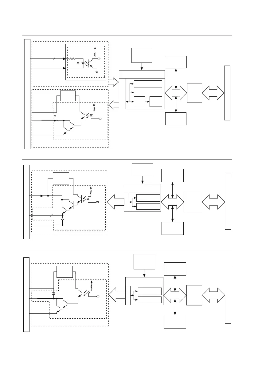
Figure 1-6. NI 6515 Block Diagram
Figure 1-7. NI 6516 Block Diagram
Figure 1-8. NI 6517 Block Diagram
PX.COM (Vcc)
PX.<0..7>
PX.GND
DO
x8 Outputs per Port
x4 Bank Isolated Digital Output Ports
PCI/PXI/CompactPCI Bus
Data/Control
PCI Bus
Interface
10 MHz
Clock
32
Digital
Outputs
32
Digital
Inputs
I/O Connector
8
PX.COM
PX.<0..7>
Vcc
x4 Bank Isolated Digital Input Ports
x8 Inputs per Port
DI
Industrial Digital
I/O Control FPGA
DIO Lines
Programmable
Power-Up States
Watchdog Timer
Change
Detection
Digital
Filtering
Data/Control
Flash
Memory
Configuration
Control
Voltage
Regulator
Industrial Digital
Output Control FPGA
Output Lines
Programmable
Power-Up States
Watchdog Timer
PCI Bus
10 MHz
Clock
Data/Control
PCI Bus
Interface
Data/Control
Flash
Memory
Configuration
Control
COM.GND
VCC
PX.<0..7>
32
DO
x32 Bank Isolated Output Channels
Voltage
Regulator
I/O Connector
32 Digital
Outputs
Industrial Digital
Output Control FPGA
Output Lines
Programmable
Power-Up States
Watchdog Timer
PCI Bus
10 MHz
Clock
Data/Control
PCI Bus
Interface
Data/Control
Flash
Memory
Configuration
Control
I/O Connector
COM (VCC)
PX.<0..7>
GND
DO
x32 Bank Isolated Output Channels
Voltage
Regulator
32 Digital
Outputs
 Loading...