3-12 | ni.com
Chapter 3 Digital I/O
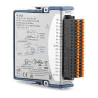
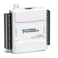
For more information on the NI 6513 signals, refer to the Signal Descriptions section.
NI 6513 R1005050 Pin Assignments
Figure 3-7 shows the pin assignments for the R1005050 cable when connecting to the NI 6513
device. The naming convention for each pin is PX.Y, where X is the port (P) number, and Y is the
line number or name.
Figure 3-7. NI 6513 Pin Assignments for the R1005050 Cable
For more information on the NI 6513 signals, refer to the Signal Descriptions section.
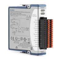
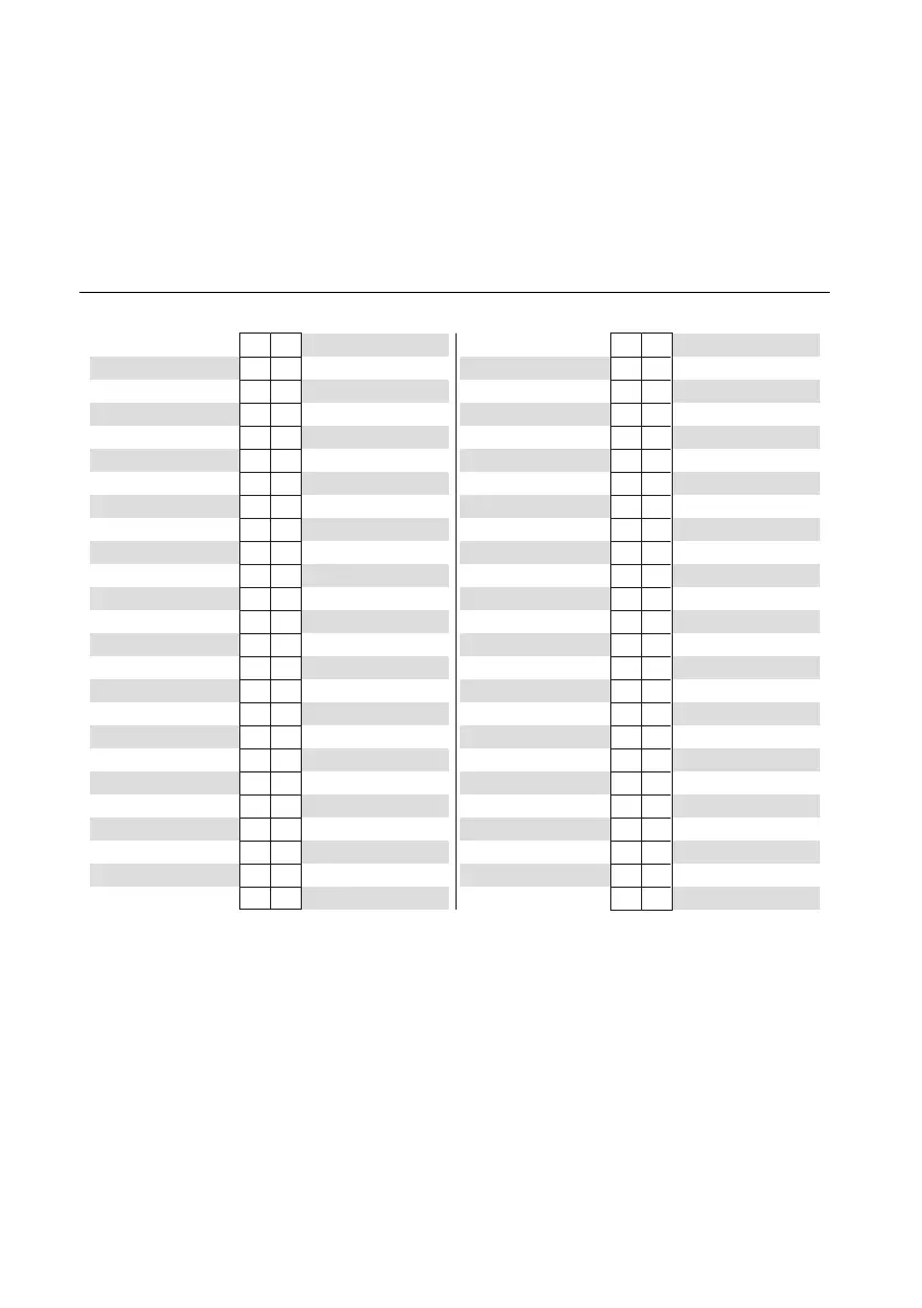
NI 6514 SH100-100-F Pin Assignments
Figure 3-8 shows the pin assignments for the SH100-100-F cable when connecting to the
NI 6514 device. The naming convention for each pin is PX.Y, where X is the port (P) number,
and Y is the line number or name.
P6.GND
P6.GND
P6.7
P6.5
P6.3
P6.1
P4.GND
P4.GND
P4.7
P4.5
P4.3
P4.1
NC
P2.GND
P2.COM (P2.VCC)
P2.6
P2.4
P2.2
P2.0
P0.GND
P0.COM (P0.VCC)
P0.6
P0.4
P0.2
P0.0
P6.+5V
P6.COM (P6.VCC)
P6.6
P6.2
P6.0
P4.GND
P4.COM (P4.VCC)
P6.GND
P6.4
P4.6
P4.4
P4.2
P4.0
P2.GND
P2.GND
P2.7
P2.5
P2.3
P2.1
P0.GND
P0.GND
P0.7
P0.5
P0.3
P0.1
49 50
47 48
45 46
43 44
41 42
3940
37 38
35 36
33 34
31 32
29 30
27 28
25 26
23 24
21 22
19 20
17 18
15 16
13 14
11 12
910
78
56
3 4
12
Positions 1 through 50 Positions 51 through 100
49 50
47 48
45 46
43 44
41 42
3940
37 38
35 36
33 34
31 32
29 30
27 28
25 26
23 24
21 22
19 20
17 18
15 16
13 14
11 12
910
78
56
3 4
12
P7.GND
P7.GND
P7.7
P7.5
P7.3
P7.1
P5.GND
P5.GND
P5.7
P5.5
P5.3
P5.1
NC
P3.GND
P3.COM (P3.VCC)
P3.6
P3.4
P3.2
P3.0
P1.GND
P1.COM (P1.VCC)
P1.6
P1.4
P1.2
P1.0
P7.+5V
P7.COM (P7.VCC)
P7.6
P7.2
P7.0
P5.GND
P5.COM (P5.VCC)
P7.GND
P7.4
P5.6
P5.4
P5.2
P5.0
P3.GND
P3.GND
P3.7
P3.5
P3.3
P3.1
P1.GND
P1.GND
P1.7
P1.5
P1.3
P1.1
NC = No Connect
 Loading...