Circuit-, IC descriptions and list of abbreviations
EN 141DVDR615/69 9.
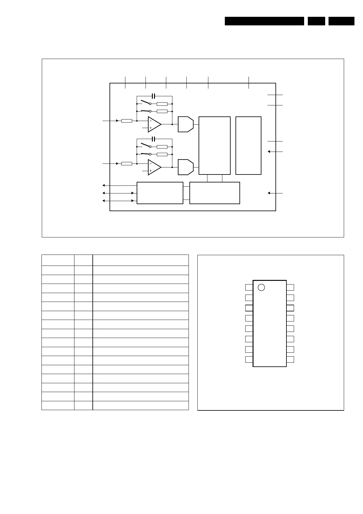
IC7006: UDA1361TS MOBO Board, Analoque to Digital Converter
Figure 9-10
BLOCK DIAGRAM
handbook, full pagewidth
UDA1361TS
MGT451
1
V
INL
ADC
Σ∆
DIGITAL
INTERFACE
DC-CANCELLATION
FILTER
DECIMATION
FILTER
CLOCK
CONTROL
3
16
V
INR
ADC
Σ∆
13
DATAO
11
BCK
12
WS
6
SFOR
7
PWON
14
MSSEL
15
10
V
SSD
9
V
DDD
V
SSA
5
V
RP
4
V
RN
2
V
ref
8
SYSCLK
V
DDA
Fig.1 Block diagram.
PINNING
SYMBOL PIN DESCRIPTION
V
INL
1 left channel input
V
ref
2 reference voltage
V
INR
3 right channel input
V
RN
4 negative reference voltage
V
RP
5 positive reference voltage
SFOR 6 data format selection input
PWON 7 power control input
SYSCLK 8 system clock 256, 384, 512 or 768f
s
V
DDD
9 digital supply voltage
V
SSD
10 digital ground
BCK 11 bit clock input/output
WS 12 word select input/output
DATAO 13 data output
MSSEL 14 master/slave select
V
SSA
15 analog ground
V
DDA
16 analog supply voltage
handbook, halfpage
UDA1361TS
MGT452
1
2
3
4
5
6
7
8
16
15
14
13
12
11
10
9
V
INL
V
ref
V
INR
V
RN
V
RP
SFOR
PWON
SYSCLK
V
DDD
V
SSD
BCK
WS
DATAO
MSSEL
V
SSA
V
DDA
Fig.2 Pin configuration.
http://www.jdwxzlw.com/?fromuser=华盛维修
 Loading...