z
zz
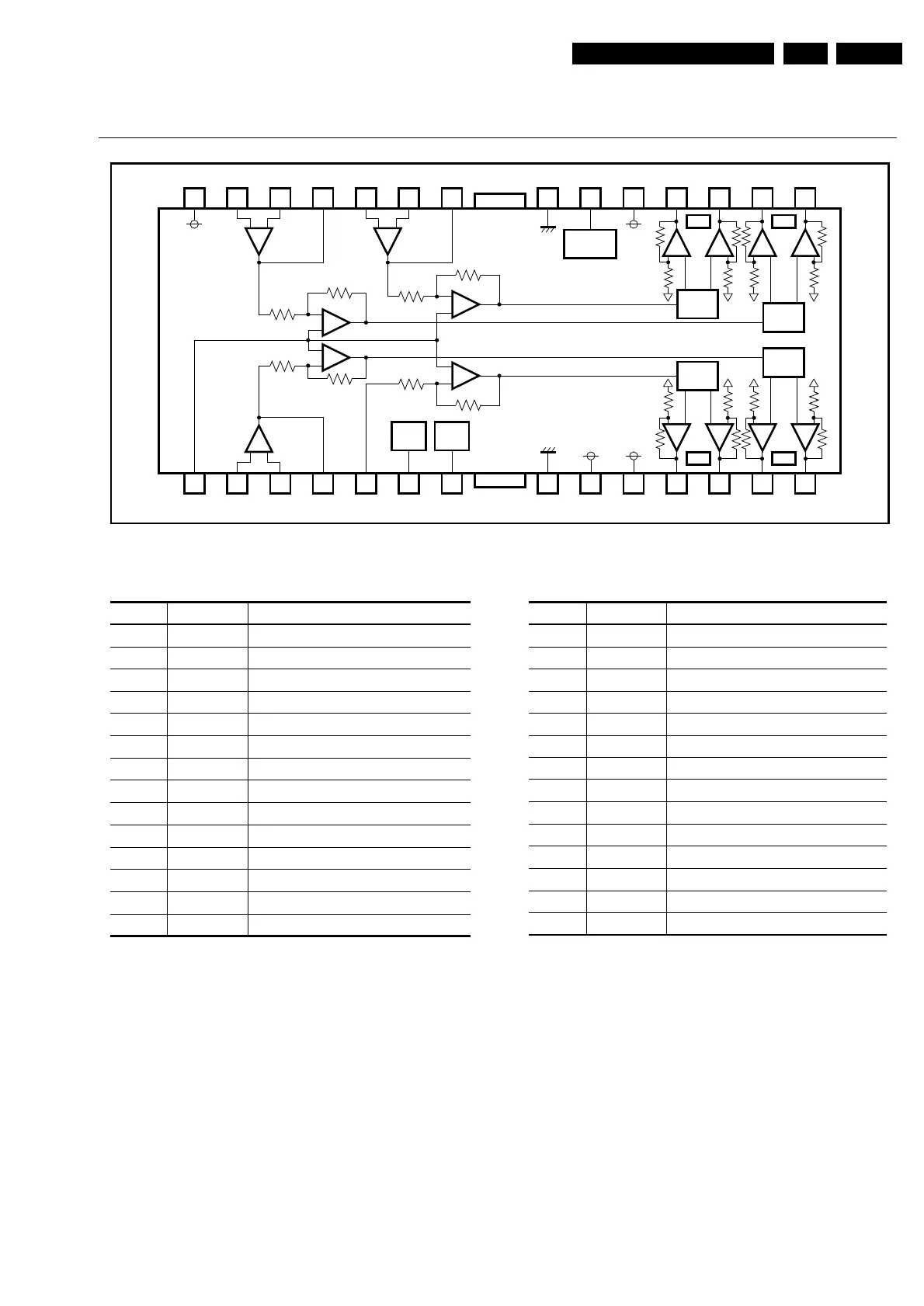
z%ORFNGLDJUDP
15
14
16
13
17
12
18
11
19
10
20
9
21
8
22
7
23
6
24
5
25
4
26
3
27
2
28
1
+
−
+
−
LEVEL
SHIFT
LEVEL
SHIFT
+
−
+
−
+
−
+
−
+
−
LEVEL
SHIFT
LEVEL
SHIFT
STAND BY
ch1 / 3 / 4
ch3
ch2
ch4
ch1
MUTE
ch1
STBY
ch2
PowV
CC
(ch3 / 4)
PowV
CC
(ch2)
PreVCC
10k10k
10k
10k
10k10k
10k
10k
10k 10k10k10k
10k 10k10k10k
20k
20k
10k
10k
+
−
20k
20k
10k
10k
+
−
+
−
+
−
+
−
+
−
+
−
PowV
CC
(ch1)
+
−
Resistor unit : [Ω]
z
zz
z3LQGHVFULSWLRQV
Pin No.
Function
1
2
3
4
5
6
7
8
9
10
11
12
13
14
BIAS IN
OPIN1 (+)
OPIN1 (−)
OPOUT1
IN2
MUTE
STBY2
GND
PowV
CC
1
PowV
CC
2
V
O2
(−)
V
O2
(+)
V
O1
(−)
V
O1
(+)
Pin No.
Pin name Function
15
16
17
18
19
20
21
22
23
24
25
26
27
28
V
O4
(+)
V
O4
(−)
V
O3
(+)
V
O3
(−)
PowV
CC
3
STBY1
GND
OPOUT3
OPIN3 (−)
OPIN3 (+)
OPOUT4
OPIN4 (−)
OPIN4 (+)
PreV
CC
Input for bias-amplifier
Non inverting input for CH1 OP-AMP
Inverting input for CH1 OP-AMP
Output for CH1 OP-AMP
Input for CH2
Input for CH1 mute control
Input for CH2 stand by control
Substrate ground
V
CC for CH1 power block
V
CC for CH2 power block
Inverted output of CH2
Non inverted output of CH2
Inverted output of CH1
Non inverted output of CH1
Non inverted output of CH4
Inverted output of CH4
Non inverted output of CH3
Inverted output of CH3
V
CC for CH3/4 power block
Input for CH1/3/4 stand by control
Substrate ground
Output for CH3 OP-AMP
Inverting input for CH3 OP-AMP
Non inverting input for CH3 OP-AMP
Output for CH4 OP-AMP
Inverting input for CH4 OP-AMP
Non inverting input for CH4 OP-AMP
V
CC for pre block
Note) Symbol of + and − (output of drivers) means polarity to input pin.
Pin name
 Loading...