Circuit-, IC descriptions and list of abbreviations
EN 161DVDR615/69 9.
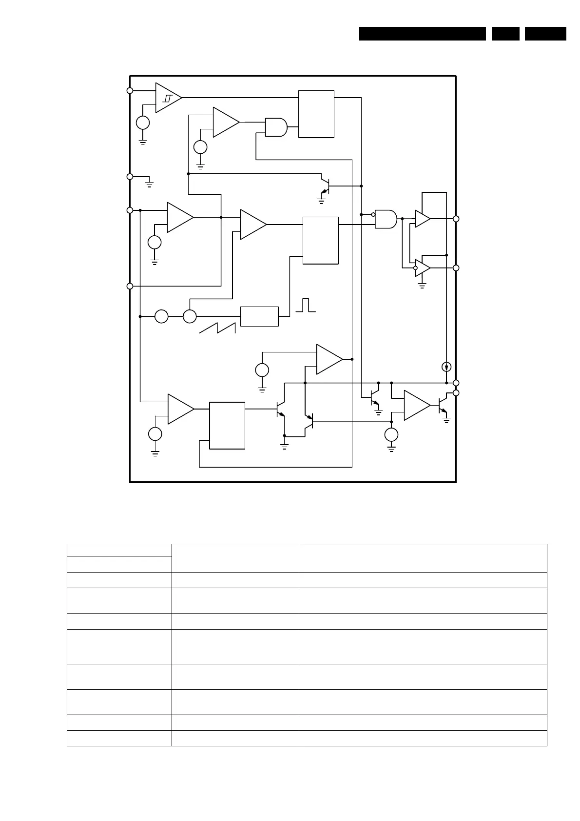
IC7929 NCP1570D, FEBE Board, DC/DC Converter Control
Figure 9-34
Figure 9-35
–
+
UVLO COMP
–
+
–
+
–
+
Fault Latch
Set Dominant
+
–
0.25 V
Error Amp
–
R
S
Q
PWM Latch
Reset Dominant
PWM COMP
+
Σ
OSC
Art Ramp
80%, 200 kHz
0.525 V
+
–
8.5 V/7.5 V
+
–
0.985 V
S
R
Q
V
CC
GND
V
FB
COMP
GATE(H)
GATE(L)
PGDELAY
PWRGD
Non
Overlap
V
CC
+
–
0.89 V/0.69 V
+
–
+
–
0.25 V
S
R
Q
PGDELAY Latch
Set Dominant
–
+
+
–
3.3 V
12 µA
+
–
PACKAGE PIN DESCRIPTION
PACKAGE PIN #
SO–8
PIN SYMBOL FUNCTION
1 V
CC
Power supply input.
2 PWRGD Open collector output goes low when V
FB
is out of regulation. User
must externally limit current into this pin to less than 20 mA.
3 PGDELAY External capacitor programs PWRGD low–to–high transition delay.
4 COMP Error amp output. PWM comparator reference i nput. A capacitor to
LGND provides error amp compensation and S oft Start. Pulling pin
< 0.45 locks gate outputs to a zero percent duty cycle state.
5 GATE(H) High–side switch FET driver pin. Capable of delivering peak currents
of 1.5 A.
6 GATE(L) Low–side synchronous FET driver pin. Capable of delivering peak
currents of 1.5 A.
7 V
FB
Error amplifier and PWM comparator i nput.
8 GND Power supply return.
http://www.jdwxzlw.com/?fromuser=华盛维修
 Loading...