ATA Bus Interface and ATA Commands
Quantum Fireball Plus AS 10.2/20.5/30.0/40.0/60.0 GB AT 6-21
6.5
6.56.5
6.5 REGISTER ADDRESS DECODING
REGISTER ADDRESS DECODINGREGISTER ADDRESS DECODING
REGISTER ADDRESS DECODING
The host addresses the drive by using programmed I/O. Host address lines A0–A2,
chip-select CS1FX– and CS3FX–, and IOR– and IOW– address the disk registers.
Host address lines A3–A9 generate the two chip-select signals, CS1FX– and
CS3FX–.
• Chip Select CS1FX– accesses the eight Command Block Registers.
• Chip Select CS3FX– is valid during 8-bit transfers to or from the
Alternate Status Register.
The drive selects the primary or secondary command block addresses by setting
Address bit A7.
Data bus lines 8–15 are valid only when IOCS16– is active and the drive is
transferring data. The drive transfers ECC information only on data bus lines 0–7.
Data bus lines 8–15 are invalid during transfers of ECC information.
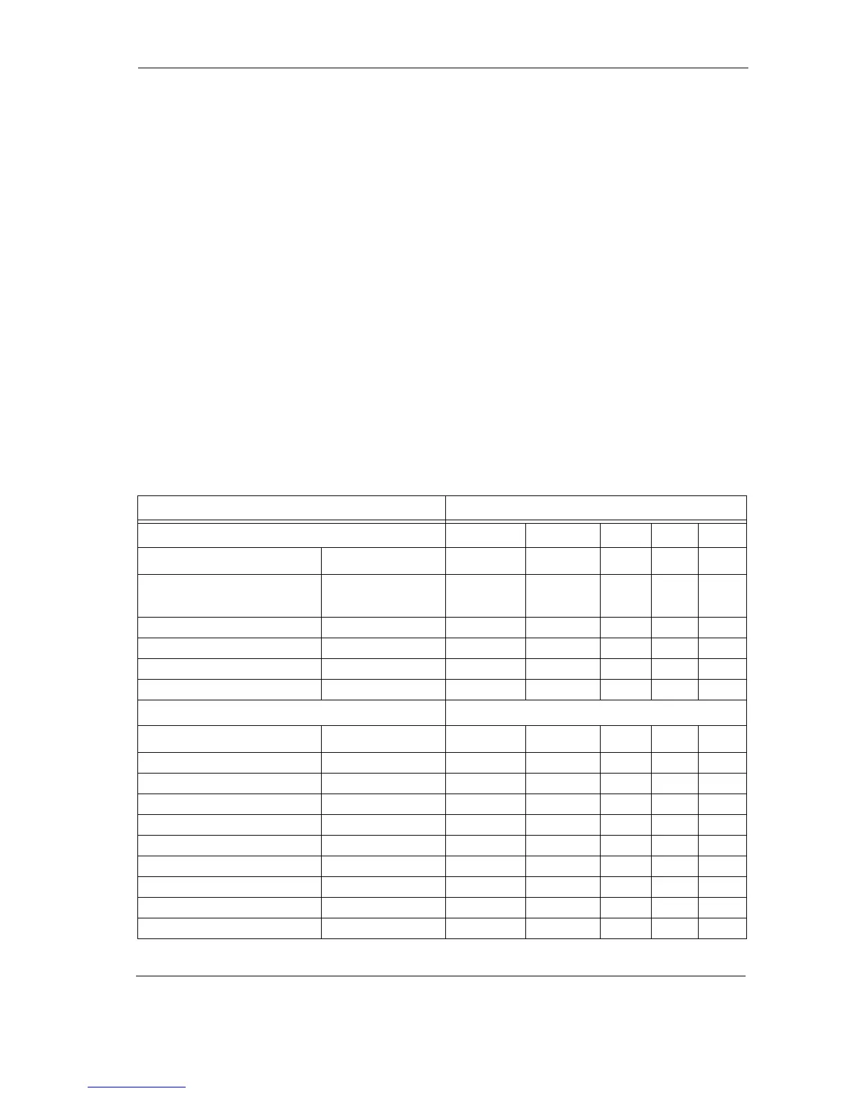
I/O to or from the drive occurs over an I/O port that routes input or output data to
or from selected registers, by using the following encoded signals from the host:
CS1FX–, CS3FX–, DA2, DA1, DA0, DIOR–, and DIOW–. The host writes to the
Command Block Registers when transmitting commands to the drive, and to the
Control Block Registers when transmitting control, like a software reset. Table 6-10
lists the selection addresses for these registers.
Table 6-10
Table 6-10 Table 6-10
Table 6-10
I/O Port Functions and Selection Addresses
FUNCTION
FUNCTIONFUNCTION
FUNCTION HOST SIGNALS
HOST SIGNALSHOST SIGNALS
HOST SIGNALS
CONTROL BLOCK REGISTERS
CONTROL BLOCK REGISTERSCONTROL BLOCK REGISTERS
CONTROL BLOCK REGISTERS CS1FX–
CS1FX–CS1FX–
CS1FX– CS3FX–
CS3FX–CS3FX–
CS3FX– DA2
DA2DA2
DA2 DA1
DA1DA1
DA1 DA0
DA0DA0
DA0
READ (DIOR–)
READ (DIOR–)READ (DIOR–)
READ (DIOR–) WRITE (DIOW–)
WRITE (DIOW–)WRITE (DIOW–)
WRITE (DIOW–)
Data Bus High
Data Bus High Data Bus High
Data Bus High
Impedance
ImpedanceImpedance
Impedance
Not Used
Not UsedNot Used
Not Used N
NN
N
1
11
1
N
NN
NX
XX
X
2
22
2
X
XX
XX
XX
X
Data Bus High Impedance Not Used N A
3
0XX
Data Bus High Impedance Not Used N A 1 0 X
Alternate Status Device Control N A 1 1 0
Drive Address Not Used N A 1 1 1
COMMAND BLOCK REGISTERS
COMMAND BLOCK REGISTERSCOMMAND BLOCK REGISTERS
COMMAND BLOCK REGISTERS
READ (DIOR–)
READ (DIOR–)READ (DIOR–)
READ (DIOR–) WRITE (DIOW–)
WRITE (DIOW–)WRITE (DIOW–)
WRITE (DIOW–)
Data Port Data Port A N 0 0 0
Error Register Features A N 0 0 1
Sector Count Sector Count A N 0 1 0
Sector Number
4
Sector Number A N 0 1 1
LBA Bits 0–7
5
LBA Bits 0–7 A N 0 1 1
Cylinder Low
4
Cylinder Low A N 1 0 0
LBA Bits 8–15
5
LBA Bits 8–15 A N 1 0 0
Cylinder High
4
Cylinder High A N 1 0 1
LBA Bits 16–23
5
LBA Bits 16–23 A N 1 0 1
 Loading...