LPWA Module Series
BG95 Hardware Design
BG95_Hardware_Design 38 / 80
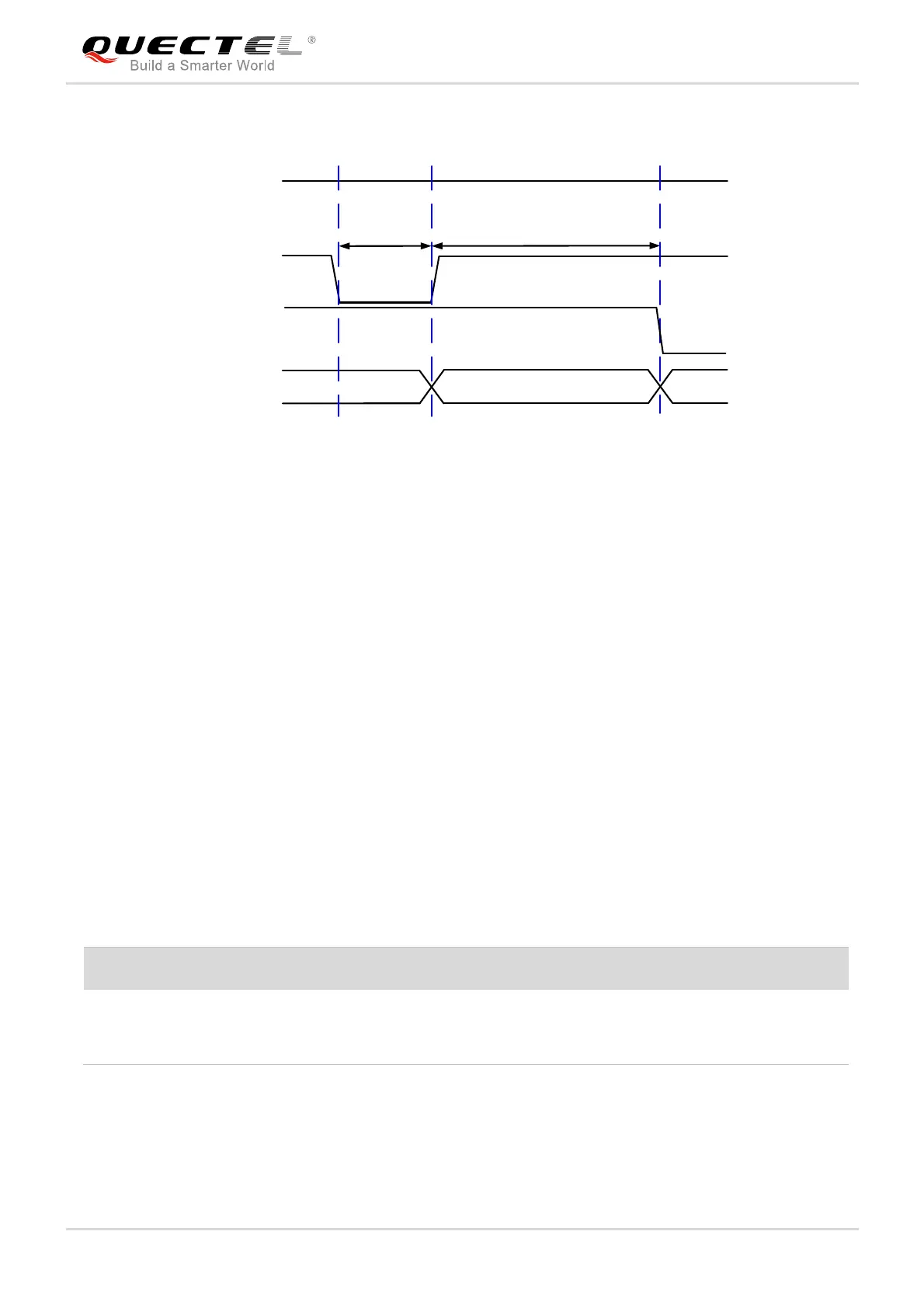
The power-down scenario is illustrated in the following figure.
VBA T
PWRKEY
TBD
650ms~150 0ms
RUNNING
Power-down procedure
OFF
Module
Status
STATUS
V
IL
≤0.45V
Figure 9: Timing of Turning off Module
3.6.2.2. Turn off Module Using AT Command
It is also a safe way to use AT+QPOWD command to turn off the module, which is similar to turning off the
module via PWRKEY pin.
Please refer to document [2] for details about AT+QPOWD
command.
3.7. Reset the Module
RESET_N is used to reset the module and will be supported in the next hardware design version. The
module can be reset by driving RESET_N to a low level voltage for a duration between 2s and 3.8s.
Table 9: Pin Definition of RESET_N
The reset scenario is illustrated in the following figure.
Pin Name Pin No. Description DC Characteristics Comment
RESET_N 17 Reset the module V
IL
max=0.45V
RESET_N will be supported in
the next hardware design
version.