EasyManuals Logo

Quectel BG95 Series User Manual

Quectel BG95 Series
84 pages
To Next Page IconTo Next Page
To Previous Page IconTo Previous Page
Page #59 background imageLoading...
Page #59 background image
LPWA Module Series
BG95 Hardware Design
BG95_Hardware_Design 58 / 80
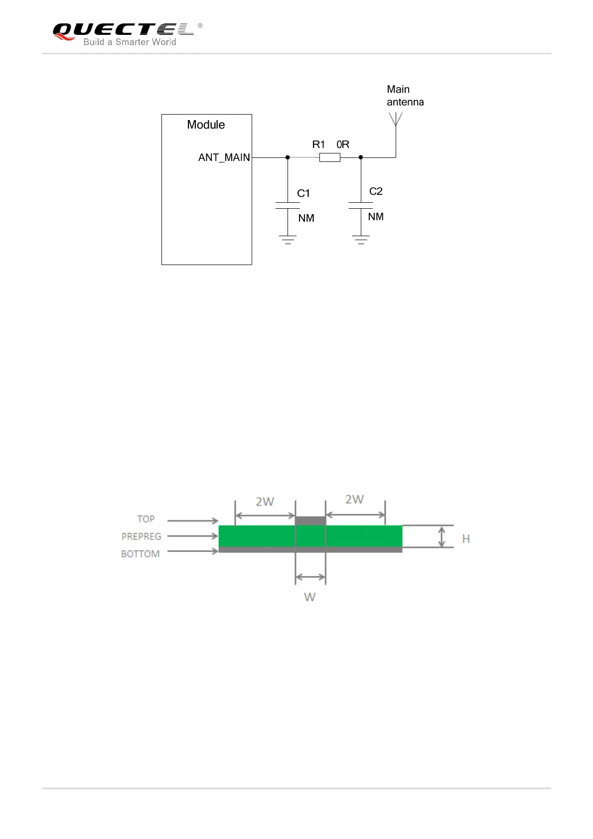
Figure 22: Reference Circuit of RF Antenna Interface
5.1.4. Reference Design of RF Layout
For user’s PCB, the characteristic impedance of all RF traces should be controlled as 50. The
impedance of the RF traces is usually determined by the trace width (W), the materials’ dielectric constant,
the distance between signal layer and reference ground (H), and the clearance between RF trace and
ground (S). Microstrip line or coplanar waveguide line is typically used in RF layout for characteristic
impedance control. The following are reference designs of microstrip line or coplanar waveguide line with
different PCB structures.
Figure 23: Microstrip Line Design on a 2-layer PCB

Table of Contents

Other manuals for Quectel BG95 Series

Questions and Answers:

Question and Answer IconNeed help?

Do you have a question about the Quectel BG95 Series and is the answer not in the manual?

Quectel BG95 Series Specifications

General IconGeneral
Form FactorLGA
Dimensions23.6 mm × 19.9 mm × 2.2 mm
Operating Temperature-40°C to +85°C
Storage Temperature-45°C to +90°C
GNSSGPS/GLONASS/BeiDou/Galileo/QZSS
SIM Interface1.8V/3.0V
LTE-FDD BandsB1/B2/B3/B4/B5/B8/B12/B13/B18/B19/B20/B26/B28
LTE-TDD BandsB39
Data rates LTE Cat NB2Uplink: 127 kbps, Downlink: 158.5 kbps
Data rates EGPRSUp to 296 kbps DL / 236.8 kbps UL
ProtocolsTCP/UDP/HTTP/HTTPS/MQTT/LWM2M/CoAP
InterfacesUART
CertificationsCE/FCC/PTCRB/IC/NCC/RCM/CCC

Related product manuals