LPWA Module Series
BG950A-GL&BG951A-GL_Hardware_Design
48
/ 84
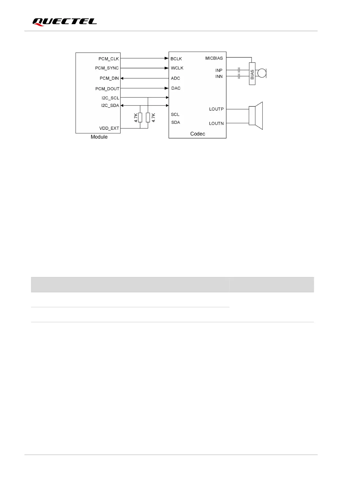
Figure 21: Reference Design of PCM Application with Audio Codec
4.5. ADC Interfaces
The module provides two Analog-to-Digital Converter (ADC) interfaces. To improve the accuracy of ADC
voltage values, the traces of ADC should be surrounded with ground.
Table 20: Pin Definition of ADC Interfaces
The voltage value on ADC pins can be read via AT+QADC=<port>:
AT+QADC=0: read the voltage value on ADC0
AT+QADC=1: read the voltage value on ADC1
For more details about the AT command, see document [3].
The resolution of the ADC is up to 12 bits. The following table describes the characteristic of the ADC
interfaces.
General-purpose ADC interface
General-purpose ADC interface

 Loading...