Single wire interface module (SWIM) UM0470
10/39 DocID14024 Rev 4
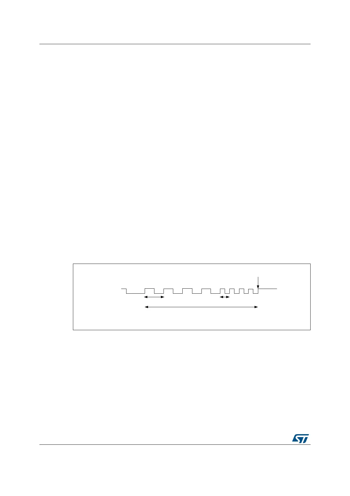
4. After this delay, the SWIM sends a synchronization frame to the host.
Synchronization frame description: a synchronization frame of 128 x SWIM clocks
periods with the SWIM line at 0 is sent out by the MCU device to allow the
measurement of the HSI by the debug host. An advanced debug host can re-calibrate
its clock to adapt to the frequency of the internal HSI RC oscillator.
5. Before starting a SWIM communication, the SWIM line must be released at 1 to
guarantee that the SWIM is ready for communication (at least 300
ns).
6. Write 0A0h in the SWIM_CSR:
- setting the bit 5 allows the whole memory range and the SRST command to be
accessed.
- setting the bit 7 masks the internal reset sources
7. Release the reset which starts the option byte loading sequence. Wait 1 ms for
stabilization.
8. Once the option byte loading has occurred and that the stabilization time is reached,
the CPU is in phase 8:
- STM8 is stalled and HSI = 16 Mhz (see STM8 datasheets for HSI clock accuracy)
- SWIM clock is at HSI/2 = 8 Mhz
- SWIM is active in low speed bit format (see Section 3.3.2)
9. After the HSI is calibrated internally, a copy of the factory calibration value is uploaded
from the option bytes and stored into the HSI calibration register at the RAM, then a
SWIM communication reset command can be generated to get the synchronization
frame again but with greater reliability than in step 4. Depending on the target context
since power on, the HSI clock could be not well calibrated in step 4, because at that
moment the HSI calibration register in the RAM is not yet initialized with the proper
value.
Figure 5. SWIM entry sequence
06Y9
6:,0SLQ
6:,0DFWLYH
PV
6:,0HQWU\VHTXHQFH
V