DocID027916 Rev 2 15/79
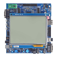
UM1902 Hardware layout and configuration
78
The led LD10 is lit when the STM32746G-EVAL evaluation board is correctly powered by
the 5 V .
Note: In order to avoid the impact of USB PHY and Ethernet PHY and get precise results of
current consumption on JP2, the following cautions need to be taken into account:
1) Configure Ethernet PHY into Power Down Mode by setting low level of IO_Expander
(EXP_IO1)
2) Configure USB HS PHY into Low Power Mode (Register Address=04,bit 6 in USB PHY).
5.3 Clock source
Two clock sources are available on STM32746G-EVAL evaluation board for
STM32F746NGH6 MCU and RTC embedded. Three clock resources for camera, Ethernet
PHY and USB OTG PHY:
• X1, 25 MHz Crystal with socket for STM32F746NGH6 Microcontroller, it can be
removed from socket when internal RC clock is used
• X2, 32 KHz Crystal for embedded RTC
• X3, 24 MHz oscillator for camera module (Default on camera daughterboard)
• X4, 25 MHz Crystal with socket for Ethernet PHY
• X5, 24 MHz Crystal for USB OTG HS PHY
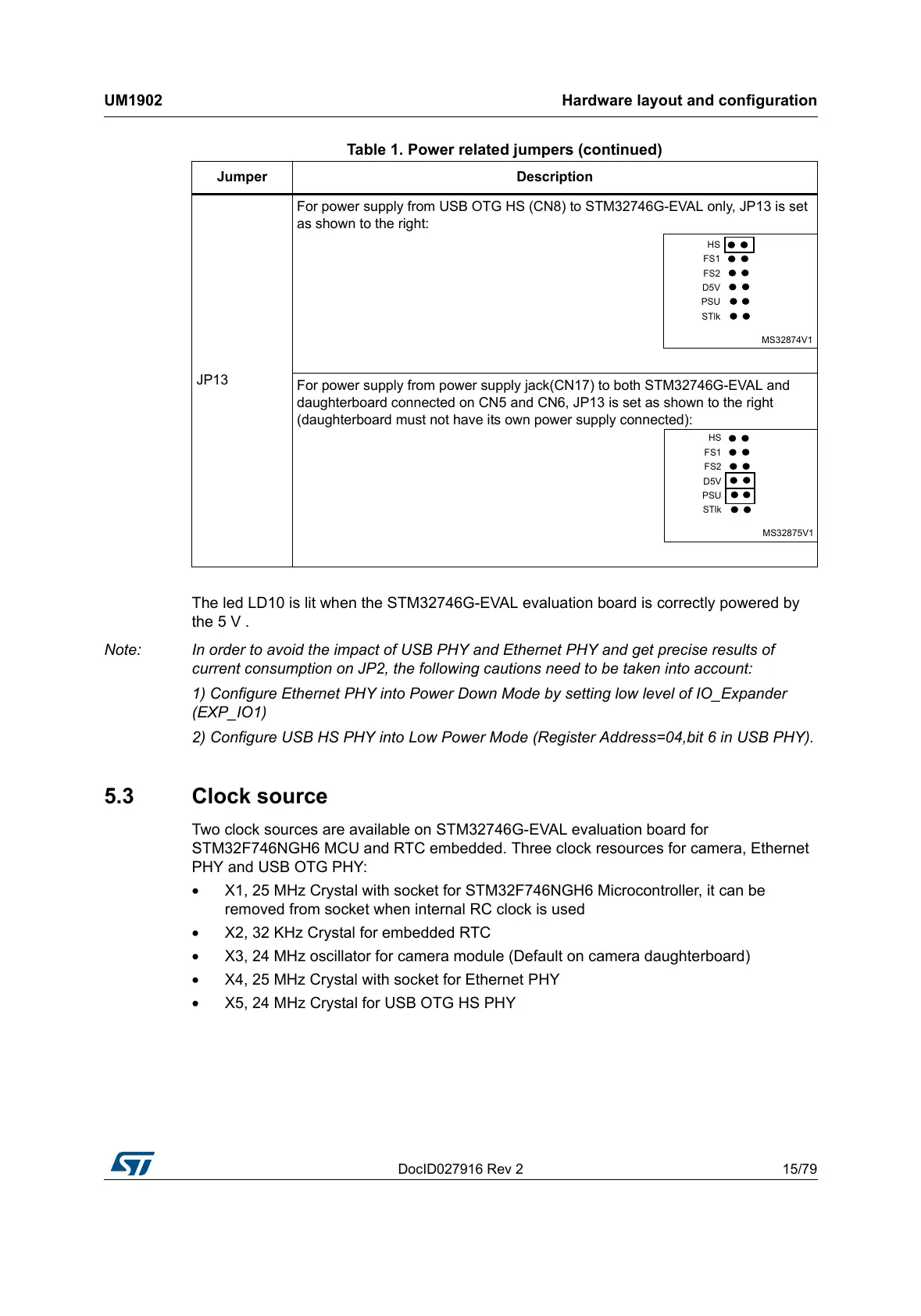
JP13
For power supply from USB OTG HS (CN8) to STM32746G-EVAL only, JP13 is set
as shown to the right:
For power supply from power supply jack(CN17) to both STM32746G-EVAL and
daughterboard connected on CN5 and CN6, JP13 is set as shown to the right
(daughterboard must not have its own power supply connected):
Table 1. Power related jumpers (continued)
Jumper Description