DocID027916 Rev 2 23/79
UM1902 Hardware layout and configuration
78
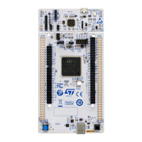
5.14 Memories
8 Mx32-bit SDRAM is connected to SDRAM Bank1 of FMC interface of the
STM32F746NGH6 microcontroller.
1 Mx16-bit SRAM is connected to bank1 NOR/PSRAM2 of FMC interface and both 8-bit and
16-bit access are allowed by BLN0 and BLN1, connected to BLE and BHE of SRAM
respectively.
A 128-Mbit Nor Flash memory is connected to the bank1 NOR/PSRAM1 of the FMC
interface. The 16-bit operation mode is selected by pull-up resistor, connected to the BYTE
pin of the NOR Flash memory. The write protection can be enabled or disabled, depending
on how the jumper JP10 is set, as showed inside Table 12.
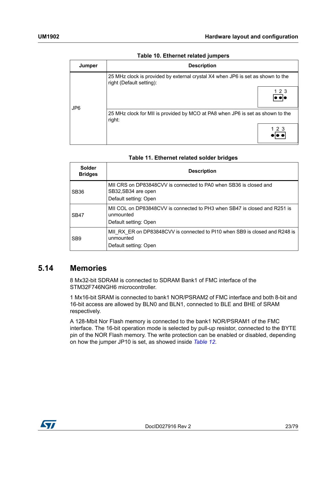
Table 10. Ethernet related jumpers
Jumper Description
JP6
25 MHz clock is provided by external crystal X4 when JP6 is set as shown to the
right (Default setting):
25 MHz clock for MII is provided by MCO at PA8 when JP6 is set as shown to the
right:
Table 11. Ethernet related solder bridges
Solder
Bridges
Description
SB36
MII CRS on DP83848CVV is connected to PA0 when SB36 is closed and
SB32,SB34 are open
Default setting: Open
SB47
MII COL on DP83848CVV is connected to PH3 when SB47 is closed and R251 is
unmounted
Default setting: Open
SB9
MII_RX_ER on DP83848CVV is connected to PI10 when SB9 is closed and R248 is
unmounted
Default setting: Open
 Loading...