DocID027916 Rev 2 9/79
UM1902 Hardware layout and configuration
78
5 Hardware layout and configuration
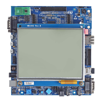
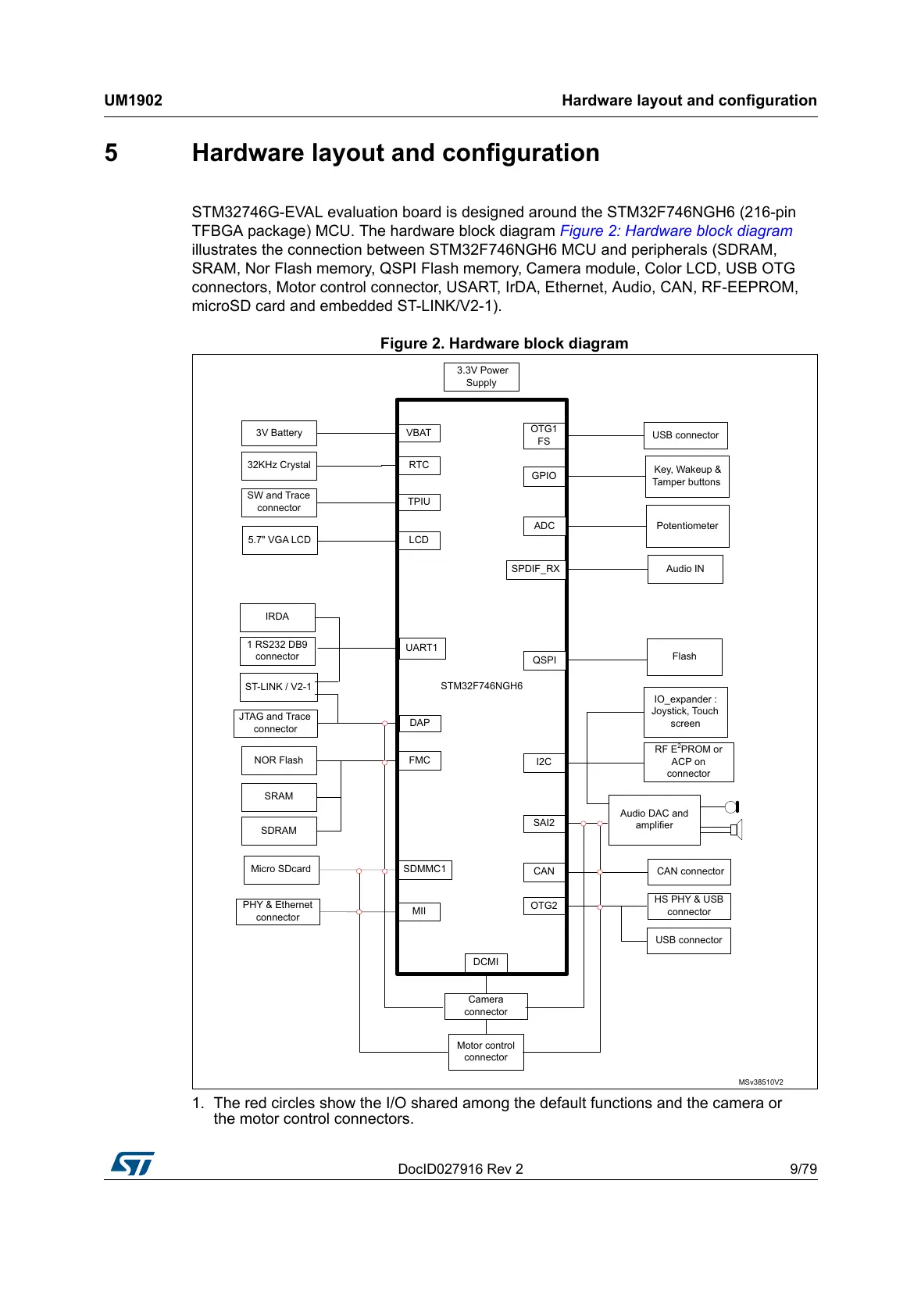
STM32746G-EVAL evaluation board is designed around the STM32F746NGH6 (216-pin
TFBGA package) MCU. The hardware block diagram Figure 2: Hardware block diagram
illustrates the connection between STM32F746NGH6 MCU and peripherals (SDRAM,
SRAM, Nor Flash memory,
QSPI Flash memory, Camera module, Color LCD, USB OTG
connectors, Motor control connector, USART, IrDA, Ethernet, Audio, CAN, RF-EEPROM,
microSD card and embedded ST-LINK/V2-1).
Figure 2. Hardware block diagram
1. The red circles show the I/O shared among the default functions and the camera or
the motor control connectors.