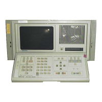
Theory of Operation
4–12
1720/1721
U774B (on Diagram 2), which has identified the +V lines (for PAL) in the
Subcarrier Regenerator.
The flip-flop outputs drive Q552 and Q553. A high output turns on the
corresponding transistor to shunt the signal at its collector to ground. This
alternately grounds and drives the + and – carrier inputs on the V Demodulator
with subcarrier to demodulate the –V lines 180° away from the +V lines.
The Chrominance Demodulators, U467 and U659, are double-balanced
demodulators, whose outputs are voltages proportional to the phase difference
between the signal input (pins 1 and 4) and the carrier input (pins 8 and 10). The
signal inputs are driven by chrominance from the Gain Cell (Diagram 1). The
carrier inputs are driven by a continuous sine wave, at subcarrier frequency, from
the Subcarrier Regenerator (Diagram 2). The subcarrier rate sine wave drives the
B–Y Demodulator directly and is delayed by 90° in the Quad Phase circuit
(L451, C451) before driving the carrier input to the B–Y Demodulator. The
V-Axis Switching circuit, when operating, determines which carrier input of the
R–Y Demodulator is driven by subcarrier.
The demodulator gains are set by the R–Y Gain (R460) and the B–Y Gain
(R655). The bias is controlled by the Center Dot Position Clamp circuits. R666
provides a small percentage of the Y signal into the X signal to be used as part of
the orthogonality adjustment.
Q353 is driven to saturation during horizontal sync time, when Q353 is saturated
any residual subcarrier present in the signal is grounded to provide a clean, zero
carrier reference for the demodulator position clamps.
A four-pole, active, low-pass filter (Q564 and Q371 for the R–Y and Q764 and
Q664 for the B–Y) removes the high-frequency components of the demodulation
process. These filters determine the bandwidth of the vector mode signal path to
control the risetime and delay of the demodulated signal.
Q570, Q571, and Q372 (for the R–Y) and Q670, Q671, and Q672 (for the B–Y)
are inverting operational amplifiers with a gain of about 15. The amplifier
outputs, to drive the Deflection Amplifiers, are from high impedance emitter
followers Q372 (R–Y) and Q670 (B–Y).
The R–Y Demodulator output is also fed back through R462 to a clamp circuit
consisting of U361 and Q362. U361 is an operational transconductance
amplifier used in a sample-and-hold circuit. The demodulated R–Y chrominance
drives the negative input (pin 2), while a voltage, controlled by the Vector
Vertical Position control (R355), is the reference level to the positive input
(pin 3).
Chrominance
Demodulators
Sync Tip Chrominance
Clamp
Demodulator Output
Filters and Amplifiers
Vector Center Dot Position
Clamp
 Loading...