WM§$XfX¥\rUlJ List of Illustrations
Figure
2-1:
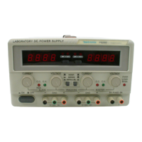
PS280 or PS283 Front Panel 2-1
Figure 2-2: Variable Power Supply Controls 2-2
Figure 2-3: Fixed Power Supply Controls 2-3
Figure 2-4: PS280 or PS283 Rear Panel 2-4
Figure
3-1:
PS280 or PS283 Variable Outputs Block Diagram 3-3
Figure 3-2: PS280 or PS283 5 V Block Diagram 3-4
Figure
4-1:
Constant Current Test Setup 4-3
Figure 4-2: Constant Current Ripple and Noise Test Setup 4-5
Figure 4-3: Constant Voltage Test Setup 4-7
Figure
5-1:
Master Circuit Board Adjustment Locations 5-8
Figure 5-2: Display Assembly Circuit Board Adjustment Locations ... 5-9
Figure 5-3: Front Panel Controls Circuit Board Adjustment Locations . 5-9
Figure
6-1:
Top Cover Removal 6-11
Figure 6-2: Slave and Fuse Circuit Board Removal 6-13
Figure 6r3: AC Selector and Master Circuit Board Removal 6-15
Figure 6^4: Front Panel Display Assembly Removal 6-18
Figure 6-5: Front Panel Controls Assembly 6-20
Figure 6-6: Output Connectors Circuit Board
and Power Switch Location 6-22
Figure 6-7: Power Transistor Circuit Boards Location 6-23
Figure
8-1:
Exploded View A 8-8
Figure 8-2: Exploded View B 8-16
PS280
&
PS283
Laboratory
DC
Power Supply
Module-Level Service Manual REV AUG 1991
vii
 Loading...