Evaluation Board Inputs and Outputs
www.ti.com
18
SNAU145B–MAY 2013–Revised March 2018
Submit Documentation Feedback
Copyright © 2013–2018, Texas Instruments Incorporated
LMK04826 and LMK04828 User’s Guide
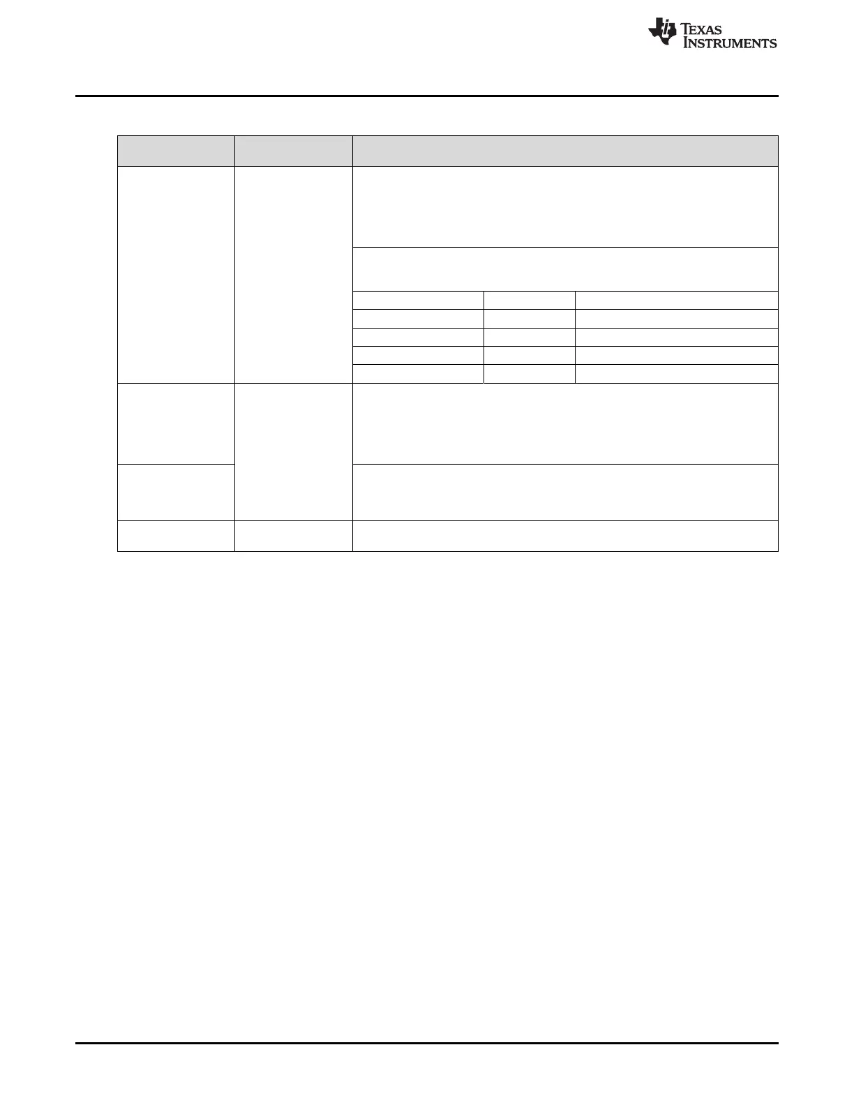
Table 5. Description of Evaluation Board Inputs and Outputs (continued)
CONNECTOR NAME
SIGNAL TYPE,
INPUT/OUTPUT
DESCRIPTION
Test points:
CLKin0_SEL_TP
CLKin1_SEL_TP
CMOS,
Input/Output
Programmable status I/O pins. By default, set as input pins for controlling input
clock switching of CLKin0 and CLKin1.
These inputs will not be functional because CLKin_SEL_MODE is set to 0 (CLKin0
Manual) by default in the User Controls page in TICS Pro. To enable input clock
switching, CLKin_SEL_MODE must be 3 and Status_CLKinX_TYPE must be 0 to 2
(pin enabled as an input).
Input Clock Switching – Pin Select Mode
When CLKin_SEL_MODE is 3, the Status_CLKinX pins select which clock input is
active as follows:
Status_CLKin1 Status_CLKin0 Active Clock
0 0 CLKin0
0 1 CLKin1
1 0 CLKin2
1 1 Holdover
Test point:
SYNC_TP
CMOS,
Input/Output
Programmable status I/O pin. By default, set as an input pin for synchronize the
clock outputs with a fixed and known phase relationship between each clock output
selected for SYNC. A SYNC event also causes the digital delay values to take
effect.
SYNC/SYSREF_REQ pin forces the SYSREF_MUX into SYSREF Continuous
mode (0x03) when SYSREF_REQ_EN = 1.
Populated:
SYNC
SYNC/SYSREF_REQ pin can hold outputs in a low state, depending on system
configuration. SYNC_POL adjusts for active low or active high control.
A SYNC event can also be programmed by toggling the SYNC_POL bit in the User
Controls page in TICS Pro.
Test point:
RESET_TP
CMOS,
Input/Output
Programmable status I/O pin.
 Loading...


