SARA-R5 series - System integration manual
UBX-19041356 - R04 Design-in Page 72 of 118
C1-Public
2.4.5 Cellular antenna detection interface (ANT_DET)
2.4.5.1 Guidelines for ANT_DET circuit design
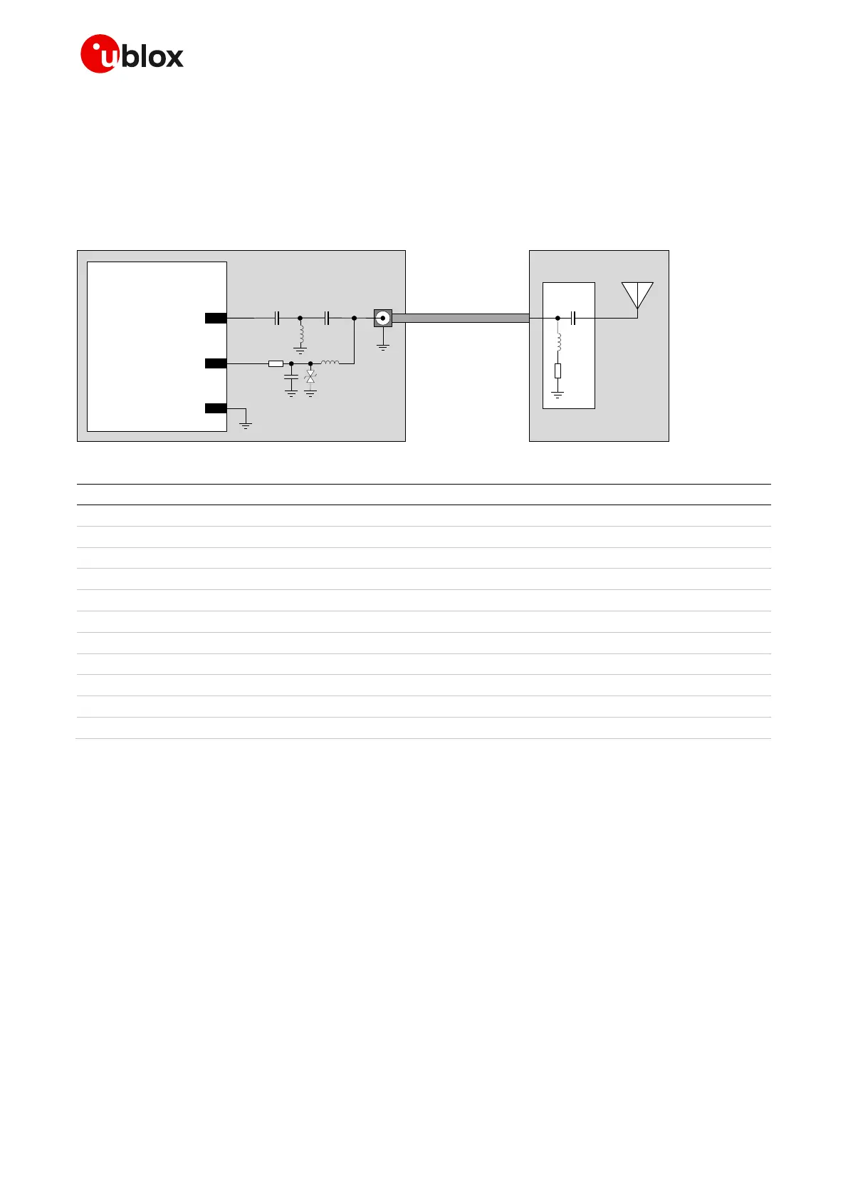
Figure 48 and Table 30 describe the recommended schematic / components for the cellular antenna
detection circuit to be provided on the application board and for the diagnostic circuit that must be
provided on the antenna’s assembly to achieve antenna detection functionality.
Application board
Antenna cable
SARA-R5 series
56
ANT
62
ANT_DET
R1
C1 D1
L1
C2
J1
Z
0
= 50
Ω
Z
0
= 50
Ω
Z
0
= 50 ohm
Antenna assembly
R2
C4
L3
Radiating
element
Diagnostic
circuit
GND
L2
C3
Figure 48: Suggested schematic for antenna detection circuit on application PCB and diagnostic circuit on antenna assembly
Part number - Manufacturer
27 pF capacitor ceramic C0G 0402 5% 50 V
GRM1555C1H270JA16 - Murata
33 pF capacitor ceramic C0G 0402 5% 50 V
GRM1555C1H330JA16 - Murata
Very low capacitance ESD protection
PESD0402-140 - Tyco Electronics
68 nH multilayer inductor 0402 (SRF ~1 GHz)
10 k resistor 0402 1% 0.063 W
SMA connector 50 through hole jack
SMA6251A1-3GT50G-50 - Amphenol
15 pF capacitor ceramic C0G 0402 5% 50 V
39 nH multilayer inductor 0402 (SRF ~1 GHz)
22 pF capacitor Ceramic C0G 0402 5% 25 V
GCM1555C1H270JA16 - Murata
68 nH multilayer inductor 0402 (SRF ~1 GHz)
15 k resistor for diagnostics
Table 30: Suggested parts for antenna detection circuit on application PCB and diagnostic circuit on antennas assembly
The antenna detection and diagnostic circuit suggested in Figure 48 and Table 30 are here explained:
• When antenna detection is forced by the +UANTR AT command (see the SARA-R5 series AT
commands manual [1]), the ANT_DET pin generates a DC current measuring the resistance (R2)
from the antenna connector (J1) provided on the application board to GND.
• DC blocking capacitors are needed at the ANT pin (C2) and at the antenna radiating element (C4)
to decouple the DC current generated by the ANT_DET pin.
• Choke inductors with a Self-Resonance Frequency (SRF) in the range of 1 GHz are needed in series
at the ANT_DET pin (L1) and in series at the diagnostic resistor (L3), to avoid a reduction of the RF
performance of the system, improving the RF isolation of the load resistor.
• Resistor on the ANT_DET path (R1) is needed for accurate measurements through the +UANTR
AT command. It also acts as an ESD protection.
• Additional components (C1 and D1 in Figure 48) are needed at the ANT_DET pin as ESD protection.
• Additional high pass filter (C3 and L2 in Figure 48) is provided as ESD immunity improvement
• The ANT pin must be connected to the antenna connector by means of a transmission line with
nominal characteristics impedance as close as possible to 50 .

 Loading...


