22 www.xilinx.com ML505/ML506/ML507 Evaluation Platform
UG347 (v3.1.1) October 7, 2009
Chapter 1: ML505/ML506/ML507 Evaluation Platform
R
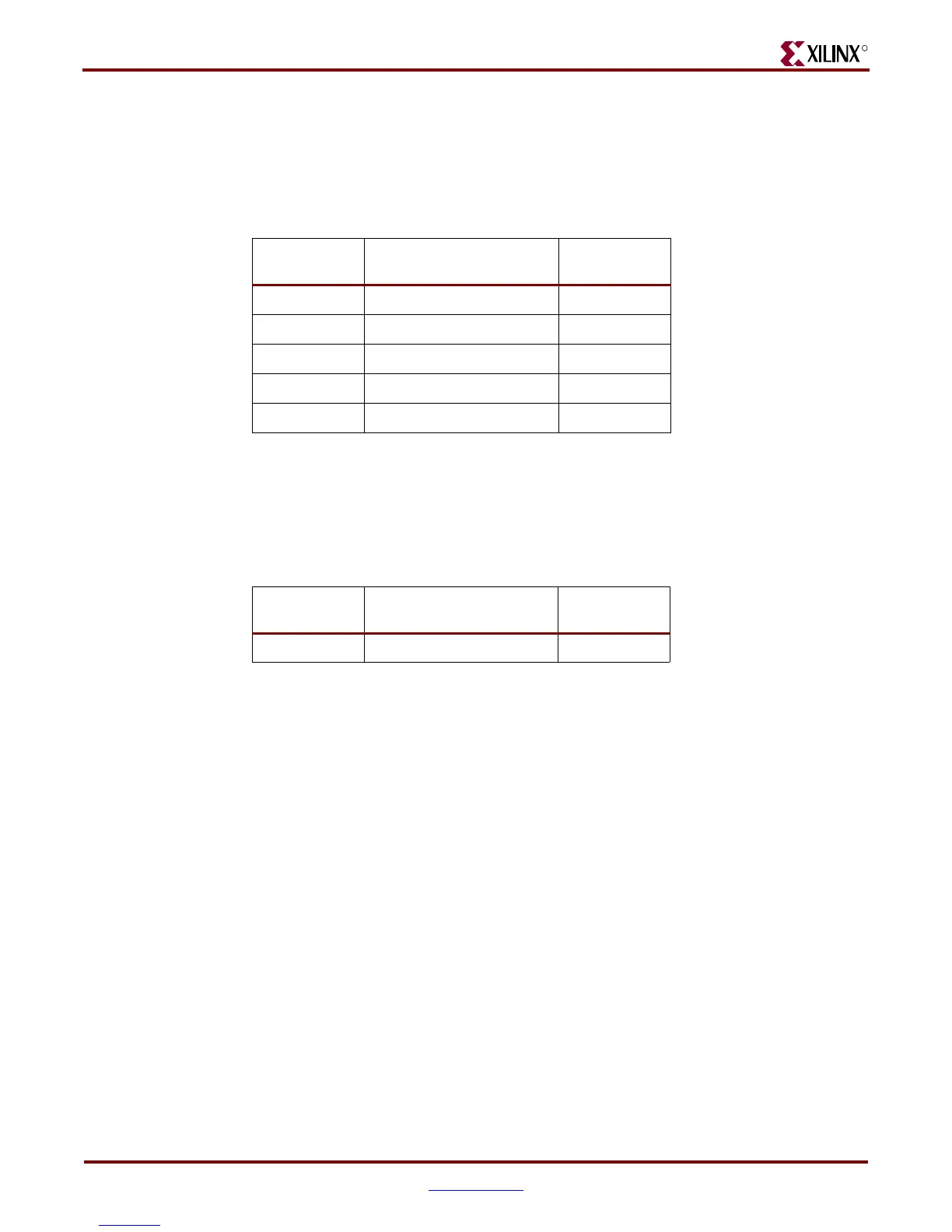
8. User Pushbuttons (Active-High)
Five active-High user pushbuttons are available for general purpose usage and are
arranged in a North-East-South-West-Center orientation (only the center one is cited in
Figure 1-2, page 15). Table 1-7 summarizes the user pushbutton connections.
9. CPU Reset Button (Active-Low)
The CPU reset button is an active-Low pushbutton and is used as a system or user reset
button. This pushbutton switch is wired only to an FPGA I/O pin so it can also be used as
a general-purpose pushbutton switch (Table 1-8).
10. XGI Expansion Headers
The board contains expansion headers for easy expansion or adaptation of the board for
other applications. The expansion connectors use standard 0.1-inch headers. The
expansion connectors contain connections to single-ended and differential FPGA I/Os,
ground, 2.5V/3.3V/5V power, JTAG chain, and the IIC bus. All signals on connectors J4
and J6 have matched length traces that are matched to each other.
Differential Expansion I/O Connectors
Header J4 contains 16 pairs of differential signal connections to the FPGA I/Os. This
permits the signals on this connector to carry high-speed differential signals, such as LVDS
data. All differential signals are routed with 100Ω differential trace impedance. Matched
length traces are used across all differential signals on J5. Consequently, these signals
connect to the FPGA I/O, and they can be used as independent single-ended nets. The
V
CCIO
of these signals can be set to 2.5V or 3.3V by setting jumper J20. Table 1-9, page 23
summarizes the differential connections on this expansion I/O connector.
Table 1-7: User Pushbutton Connections
Reference
Designator
Label/Definition FPGA Pin
SW10
N (GPIO North)
U8
SW11
S (GPIO South)
V8
SW12
E (GPIO East)
AK7
SW13
W (GPIO West)
AJ7
SW14
C (GPIO Center)
AJ6
Table 1-8: CPU Reset Connections
Reference
Designator
Label/Definition FPGA Pin
SW7 CPU RESET E9
Downloaded from Elcodis.com electronic components distributor