ML505/ML506/ML507 Evaluation Platform www.xilinx.com 49
UG347 (v3.1.1) October 7, 2009
Detailed Description
R
45. System Monitor
The ML50x supports both the dedicated and the auxiliary analog inputs to the Virtex-5
FPGA System Monitor block. The VP and VN pins shown in Table 1-34, page 50 are the
dedicated pins, whereas the VAUXP[x], VAUXN[x] represent the 16 user-selectable
auxiliary analog input channels. The ML50x PCB layout for the VP and VN pins is
designed using differential pairs and anti-alias filtering in close proximity to the FPGA as
recommended in the Virtex-5 FPGA System Monitor User Guide [Ref 14]. Please note that the
circuitry connected to the 16 AUX channels on the ML50x are connected in a non-optimal
fashion as they are implemented without anti-alias filtering at the FPGA. This tradeoff was
B2 HDR1_6 H34
B3 HDR1_8 G33
B4 GND N/A
B5 HDR1_14 J32
B6 HDR1_16 J34
B7 GND N/A
B8 HDR1_18 L33
B9 HDR1_20 M32
B10 GND N/A
B11 HDR1_26 AA34
B12 HDR1_28 AD32
B13 GND N/A
B14 HDR1_34 W32
B15 HDR1_36 AH34
B16 GND N/A
B17 HDR1_42 AH32
B18 HDR1_44 AK34
B19 GND N/A
B20 HDR2_42_SM_14_N AE34
B21 HDR2_44_SM_14_P AF34
B22 GND N/A
B23 HDR1_54 AL33
B24 HDR1_56 AM33
B25 GND N/A
B26 HDR1_62 AN34
B27 HDR1_64 AN33
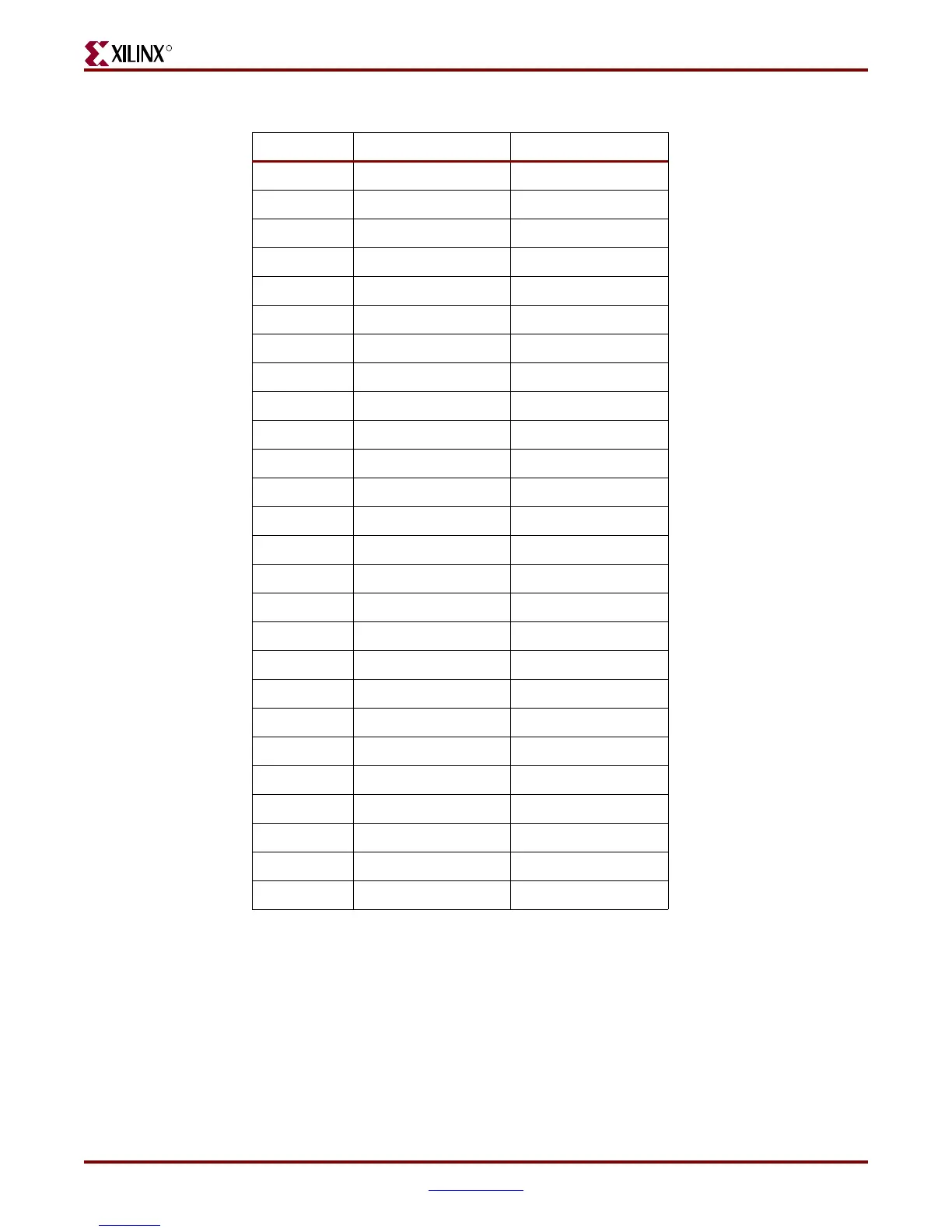
Table 1-33: Landing Pad Signals on XGI Header (Cont’d)
Pad Number Header Pin FPGA Pin
Downloaded from Elcodis.com electronic components distributor

 Loading...


