46 www.xilinx.com ML505/ML506/ML507 Evaluation Platform
UG347 (v3.1.1) October 7, 2009
Chapter 1: ML505/ML506/ML507 Evaluation Platform
R
43. GTP/GTX Clocking Circuitry
Overview
Low jitter LVDS clock sources on the board provide high-quality reference clocks for the
GTP/GTX transceivers. Different clock sources are provided to support each of the
transceiver interfaces on the board. Table 1-29 provides a summary of the GTP clock
sources. Table 1-29 provides a summary of the GTX clock sources.
Frequency Synthesizer for SFP/SMA GTP/GTX Transceiver Clocking
An Integrated Circuit Systems ICS843001-21 frequency synthesizer chip offers flexible,
low-jitter clock generation for the GTP/GTX pair connected to SFP and SMA interfaces.
The ICS843001-21 is connected to a 19.44-MHz crystal and a socketed 25-MHz oscillator
(X5).
DIP switches (SW6) enable the user to select clock source and frequency synthesis options
to generate a number of commonly used frequencies for applications, such as Gigabit
Ethern
et and SONET (see Table 1-31, page 47). For other frequencies, consult the
ICS843001-21 data sheet for more information. The 25-MHz oscillator is socketed to allow
the user to change the oscillator frequency and use the entire range of possible synthesized
frequency outputs.
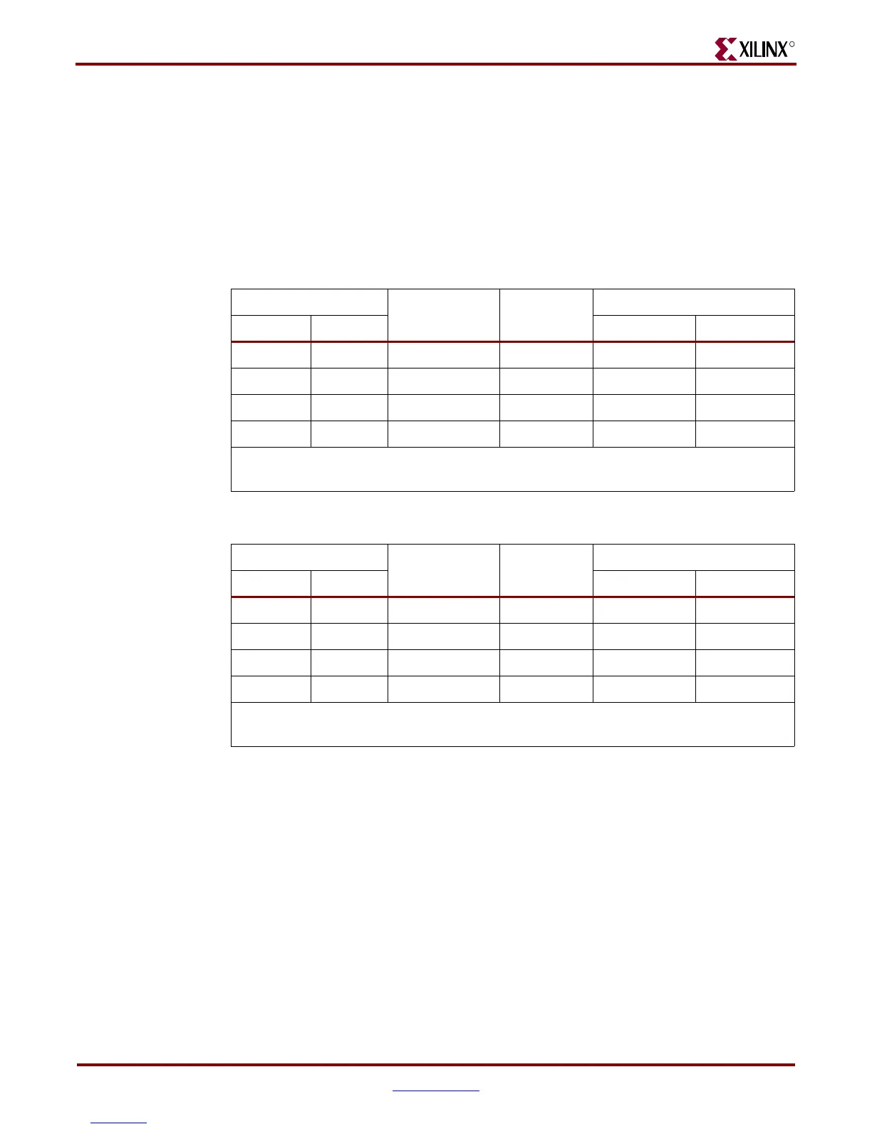
Table 1-29: GTP Clock Sources (ML505/ML506)
GTP Pairs
Frequency
GTP Tile
Location
GTP REFCLK Diff Pair
GTP0 GTP1 Positive Negative
SFP SMA Variable GTP_X0Y4 H4 H3
SATA1 SATA2 75 or 150 MHz GTP_X0Y2 Y4 Y3
SGMII Loopback 125 MHz GTP_X0Y3 P4 P3
PCIe
(1)
Loopback 100 MHz GTP_X0Y1 AF4 AF3
Notes:
1. Driven by an external PCIe source through the PCIe edge connector (P21); not driven internally.
Table 1-30: GTX Clock Sources (ML507)
GTX Pairs
Frequency
GTX Tile
Location
GTX REFCLK Diff Pair
GTX0 GTX1 Positive Negative
SFP SMA Variable GTX_X0Y5 H4 H3
SATA1 SATA2 75 or 150 MHz GTX_X0Y3 Y4 Y3
SGMII Loopback 125 MHz GTX_X0Y4 P4 P3
PCIe
(1)
Loopback 100 MHz GTX_X0Y2 AF4 AF3
Notes:
1. Driven by an external PCIe source through the PCIe edge connector (P21); not driven internally.
Downloaded from Elcodis.com electronic components distributor