ML505/ML506/ML507 Evaluation Platform www.xilinx.com 53
UG347 (v3.1.1) October 7, 2009
Configuration Options
R
Configuration Options
The FPGA on the ML50x Evaluation Platform can be configured by the following major
devices:
• Xilinx download cable (JTAG)
• System ACE controller (JTAG)
• Two Platform Flash PROMs
• Linear Flash memory
• SPI Flash memory
The following section provides an overview of the possible ways the FPGA can be
configured.
JTAG (Xilinx Download Cable and System ACE Controller) Configuration
The FPGA, two Platform Flash PROMs, and CPLD can be configured through the JTAG
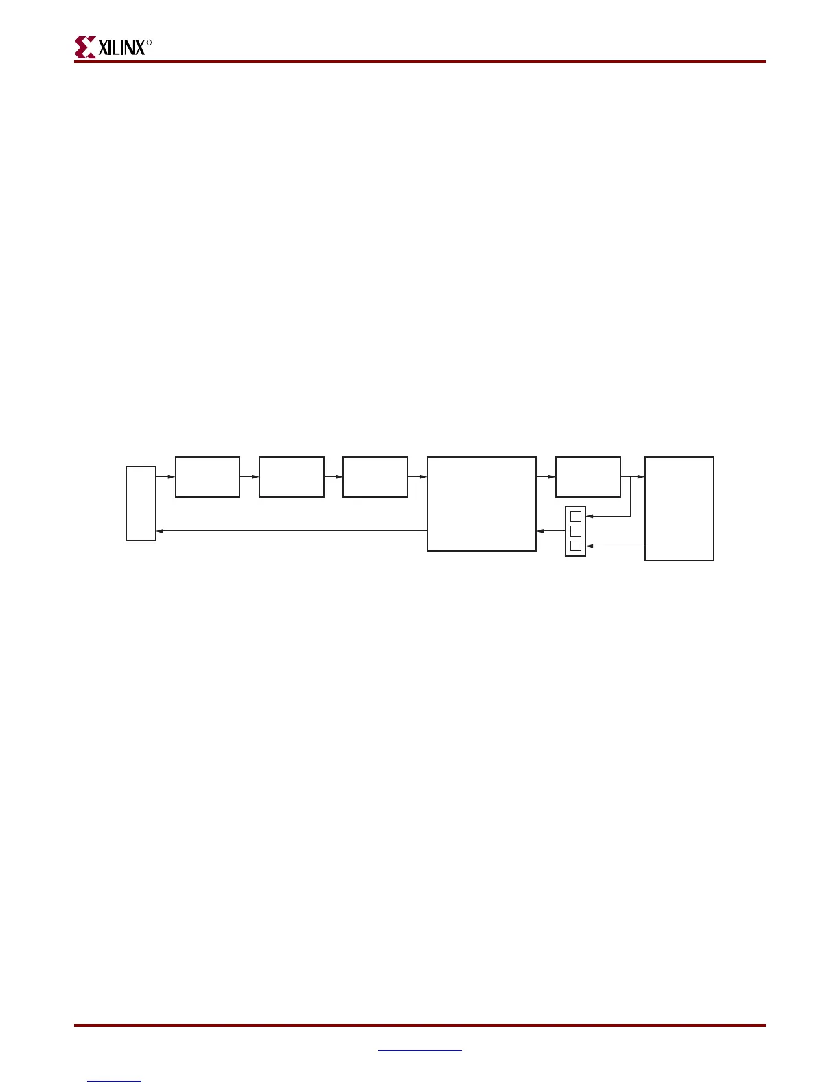
port. The JTAG chain of the board is illustrated in Figure 1-9.
The chain starts at the PC4 connector and goes through the Platform Flash PROMs, the
CPLD, the System ACE controller, the FPGA, and an optional extension of the chain to the
expansion card. Jumper J21 determines if the JTAG chain should be extended to the
expansion card.
The JTAG chain can be used to program the FPGA and access the FPGA for hardware and
software debug. The JTAG chain is also used to program the Platform Flash PROM and the
CPLD.
The PC4 JTAG connection to the JTAG chain allows a host computer to download
bitstreams to the FPGA using the iMPACT software tool. PC4 also allows debug tools such
as the ChipScope Pro Analyzer or a software debugger to access the FPGA.
The System ACE controller can also program the FPGA through the JTAG port. Using an
inserted CompactFlash card, configuration information can be stored and played out to
the FPGA. The System ACE controller supports up to eight configuration images that can
selected using the three configuration address DIP switches. Under FPGA control, the
System ACE chip can be instructed to reconfigure to any of the eight configuration images.
The configuration mode should be set to 101. Jumper J21 should exclude the expansion
card from the JTAG chain, and switch SW3, pin 8 should be ON to use System ACE
configuration. When set correctly, the System ACE controller programs the FPGA upon
power-up if a CompactFlash card is present or whenever a CompactFlash card is inserted.
Figure 1-9: JTAG Chain
UG347_08_112706
System ACE
Controller
TSTTDI
TSTDO
CFGTDO
CFGTDI
PC4
Connector
FPGA
J21
J1
TDI
1
2
3
TDO
Expansion
TDI
TDO
Platform Flash Memories CPLD
TDI TDO TDI TDO
U4 U5 U3
U2
U1
J5
TDI TDO
Downloaded from Elcodis.com electronic components distributor

 Loading...


