16 www.xilinx.com ML605 Hardware User Guide
UG534 (v1.9) February 26, 2019
Chapter 1: ML605 Evaluation Board
1. Virtex-6 XC6VLX240T-1FFG1156 FPGA
A Virtex-6 XC6VLX240T-1FFG1156 FPGA is installed on the embedded development
board.
Keep-Out areas and drill holes are defined around the FPGA to support an Ironwood
Electronics SG-BGA-6046 FPGA socket.
See the Virtex-6 FPGA Data Sheet (DS152). [Ref 4]
Configuration
The ML605 supports configuration in the following modes:
• Slave SelectMAP (using Platform Flash XL with the onboard 47 MHz oscillator)
• Master BPI-Up (using Linear BPI Flash device)
• JTAG (using the included USB-A to Mini-B cable)
•JTAG (using System ACE CF and CompactFlash card)
The ML605 supports Master BPI-Up, JTAG, and Slave SelectMAP. These are selected by
setting M[2:0] options 010, 101 and 110 shown in Table 1-2.
For an overview on configuring the FPGA, see Configuration Options.
Note:
The mode switches are part of DIP switch S2. The default mode setting (see Table A-34) is
M[2:0]=010, which selects Master BPI-Up at board power-on. Switch S1 position 4 must be OFF to
disable the System ACE controller from attempting to boot if a CF card is present.
See the Virtex-6 FPGA Configuration User Guide (UG360) for detailed configuration
information. [Ref 5]
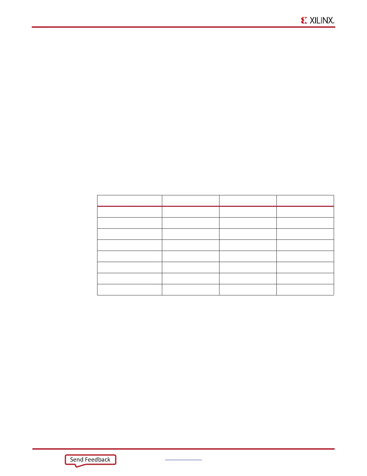
Table 1-2: Virtex-6 FPGA Configuration Modes
Configuration Mode M[2:0] Bus Width
(1)
CCLK Direction
Master Serial
(2)
000 1Output
Master SPI
(2)
001 1Output
Master BPI-Up
(2)
010 8, 16 Output
Master BPI-Down
(2)
011 8, 16 Output
Master SelectMAP
(2)
100 8, 16 Output
JTAG 101 1 Input (TCK)
Slave SelectMAP 110 8, 16, 32 Input
Slave Serial
(3)
111 1 Input
Notes:
1. The parallel configuration modes bus is auto-detected by the configuration logic.
2. In Master configuration mode, the CCLK pin is the clock source for the Virtex-6 FPGA internal
configuration logic. The Virtex-6 FPGA CCLK output pin must be free from reflections to avoid
double-clocking the internal configuration logic. See the Virtex-6 FPGA Configuration User Guide for
more details. [Ref 5]
3. This is the default setting due to internal pull-up termination on mode pins.

 Loading...


