80 www.xilinx.com ML605 Hardware User Guide
UG534 (v1.9) February 26, 2019
Appendix A: Default Switch and Jumper Settings
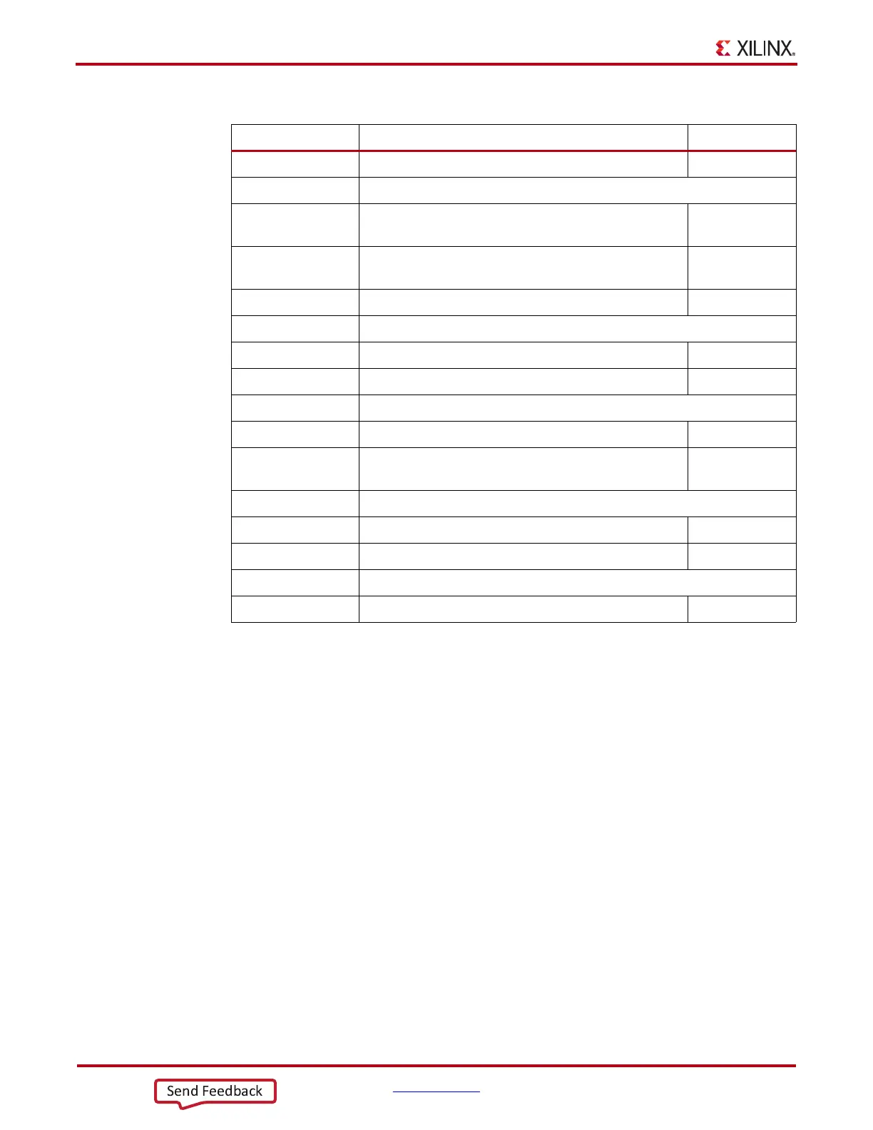
Table A-35: Default Jumper Settings
Jumper REFDES Function Default
J69 System ACE CF Error LED Enable Jump 1-2
GMII:
J66
pins 1-2: GMII/MII to Cu
pins 2-3: SGMII to Cu, no clk
Jump 1 - 2
J67
pins 1-2: GMII/MII to Cu
pins 2-3: SGMII to Cu, no clk
Jump 1 - 2
J68 J66 pins 1-2, J68 ON: RGMII, modified MII in Cu no jumper
FMC JTAG Bypass:
J18 exclude FMC LPC connector Jump 1 - 2
J17 exclude FMC HPC connector Jump 1 - 2
System Monitor:
J19 Test_mon_vrefp sourced by U23, REF3012 Jump 1 - 2
J35 measure voltage across R-kelvin on VCCINT
Jump 9 - 11,
Jump 10 - 12
SFP Module:
J54 Full BW Jump 1 - 2
J65 SFP Enable Jump 1 - 2
PCIe Lane Size:
J42 1 lane Jump 1 - 2

 Loading...


