30 www.xilinx.com ML605 Hardware User Guide
UG534 (v1.9) February 26, 2019
Chapter 1: ML605 Evaluation Board
The JTAG chain can be used to program the FPGA and access the FPGA for hardware and
software debug.
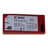
The JTAG connector (USB Mini-B J22) allows a host computer to download bitstreams to
the FPGA using the Xilinx iMPACT software tool. In addition, the JTAG connector allows
debug tools such as the ChipScope™ Pro Analyzer tool or a software debugger to access
the FPGA. The iMPACT software tool can also program the BPI flash via the USB J22
connection. iMPACT can download a temporary design to the FPGA through the JTAG.
This provides a connection within the FPGA from the FPGA's JTAG port to the FPGA's BPI
interface. Through the connection made by the temporary design in the FPGA, iMPACT
can indirectly program the BPI flash or the Platform Flash XL from the JTAG USB J22
connector.
For an overview on configuring the FPGA, see Configuration Options.
7. Clock Generation
There are three FPGA fabric clock sources available on the ML605 (refer to Table 1-7).
Oscillator (Differential)
The ML605 has one 2.5V LVDS differential 200 MHz oscillator (U11) soldered onto the
board and wired to an FPGA global clock input. The 200 MHz signal names are
SYSCLK_N and SYSCLK_P.
• Crystal oscillator: SiTime SiT9102AI-243N25E200.00000
• Frequency stability: 50 ppm
For more details, see the SiTime SiT9102 data sheet [Ref 28]. For more information about
LVDS clocking, refer to
Virtex-6 FPGA Data Sheet (DS152) [Ref 4].
Oscillator Socket (Single-Ended, 2.5V)
One populated single-ended clock socket (X5) is provided for user applications. The X5
socket is populated with a 66 MHz 2.5V single-ended MMD Components MBH2100H-
66.000 MHz oscillator. The 66 MHz signal name is USER_CLOCK.
For more information about LVDS clocking, refer to
Virtex-6 FPGA Data Sheet (DS152)
[Ref 4].
 Loading...
