EasyManuals Logo
Home>Xinje>Inverter>VB5N Series

Xinje VB5N Series User Manual

Xinje VB5N Series
105 pages
To Next Page IconTo Next Page
To Previous Page IconTo Previous Page
Page #76 background imageLoading...
Page #76 background image
VB5N series inverter
68
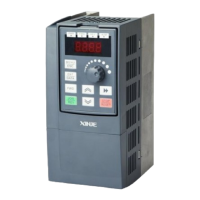
Fig 4-26 Frequency arriving signal
P4.13
FDT1 (frequency level) voltage
Range: 0.00~upper limit of frequency
10.00Hz
P4.14
FDT1 lag
Range: 0.00~50.00Hz
1.00Hz
P4.15
FDT2 (frequency level) voltage
Range: 0.00~upper limit of frequency
10.00Hz
P4.16
FDT2 lag
Range: 0.00~50.00Hz
1.00Hz
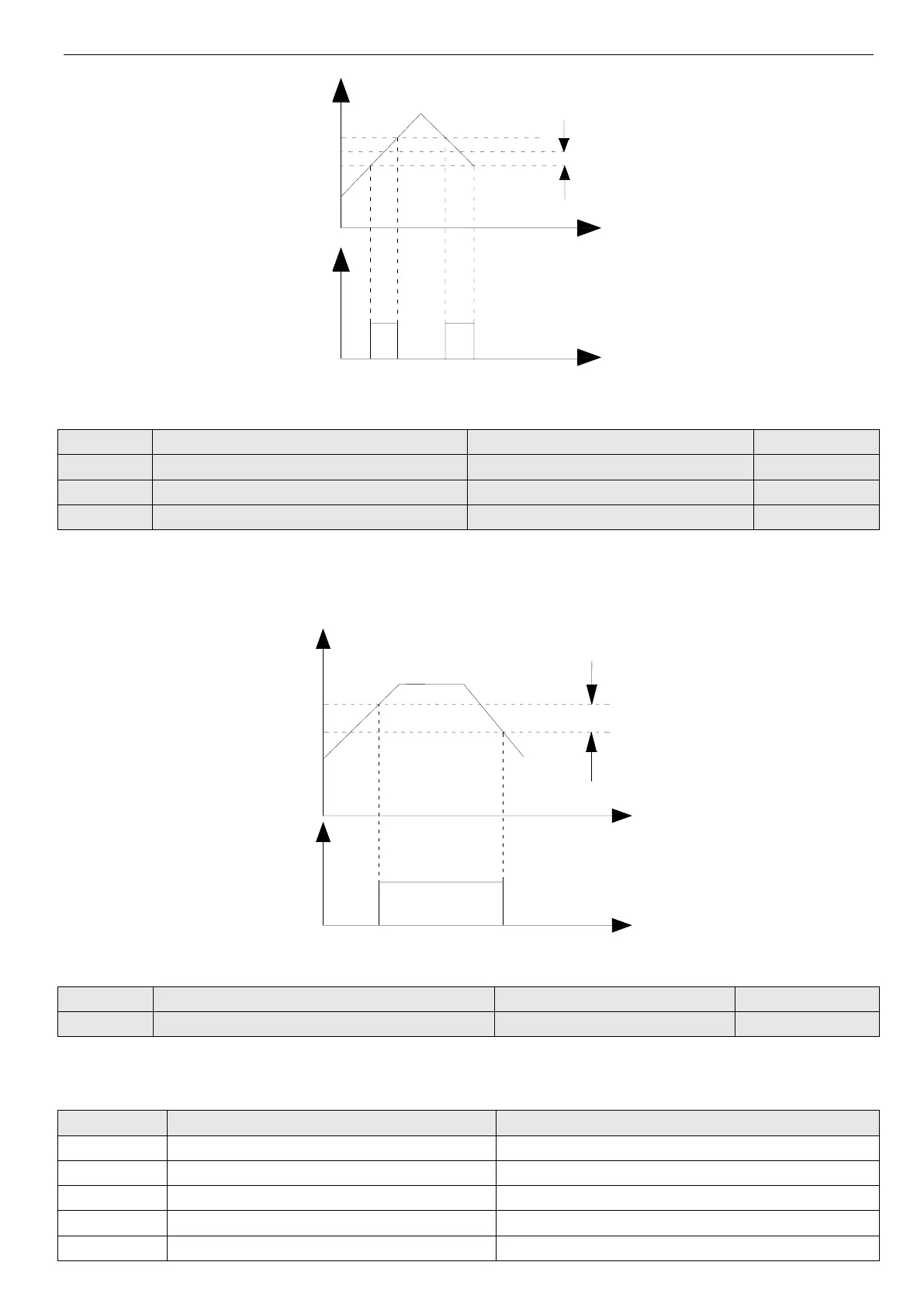
P4.13~P4.14 is the additional definition of No.2 function in Table.4-6, P4.15~P4.16 is the additional definition of No.3
function in Table.4-6, their using method are the same. The following takes P4.13~P4.14 as an example to introduce.When
the output frequency is over one frequency(FDT1 voltage), indication signal will be output until the output frequency de-
creasing below one frequency of FDT1(FDT1 voltageFDT1 lag), as shown in Fig. 4-27.
Fig.4-27 FDT level
P4.17
Analog output selection (AO)
Range: 0~7
0
P4.18
Analog output gain (AO)
Range: 0.50~2.00
1.00
Table 4-7 Output terminals
No.
Function
Range
0
Output frequency
0~upper limit frequency
1
Output current
0~2 × rated current
2
Output voltage
0~1.2 × rated voltage of load motor
3
Bus voltage
0~800V
4
PID setting
0~10V
Time
Time
Y
FDT1 voltage
FDT1 lag
Set frequency
Output
Checking range
Time
Time
Y
Output frequency

Table of Contents

Questions and Answers:

Question and Answer IconNeed help?

Do you have a question about the Xinje VB5N Series and is the answer not in the manual?

Xinje VB5N Series Specifications

General IconGeneral
BrandXinje
ModelVB5N Series
CategoryInverter
LanguageEnglish

Related product manuals