4-6
W300
+8
REG
PWR
CTRL
UT8
VCC
SW
CPU3.3V
5V
PCON
REG
REG
3VS
5VS
FANHV
REG
IDET
DETECT
CURRENT
NOISE
FILTER
REG
VT8
REG
3.3V
UTX_C
VTX_C
I SENS
3.3V
CTRL8V
REG
8V
BT3.3V
BT3V
REG
UT8
VT8
HV
CONT8V
SW
REG(6V)
PSC
SW
SD3V
REG
SD3.3V
LOW V
DET
PDV
ALARM
To BT
To CPU
REG
4.2V
CAP
SUPER
MAIN UNIT
IC310
Q302/Q306
IC313
Q301
IC309
IC320
IC305
IC306
IC311
IC323 C1340
IC314
IC319Q303
IC321
Q32/Q34
Q27/Q28
IC403
3.3V
REG
IC404
1.3V
REG
DSP3.3V
DSP1.3V
VCC
IC324
Ball
No.
Line Name Description I/O
7 TWDTX
Touch panel controller touch sens-
ing data.
O
14 RESET Reset signal input. I
15 R_VOLV Band B [VOL] input. I
16 R_SQLV Band B [SQL] input. I
17 L_VOLV Band A [VOL] input. I
18 L_SQLV Band A [SQL] input. I
25 G_TXD
GPS data.
O
26 G_RXD I
29 DIM_DA LCD backlit brightness control. O
30 G_RES
GPS module (EP13) reset.
L= Resets.
O
31 GPSC
GPS module (EP13) power supply
control.
L=GPS module is activated.
O
32 LCDRST
LCD controller reset.
L= Resets.
O
33 TEMP
LCD controller temperature sens-
ing voltage.
I
38–
41
LCDD4–
LCDD7
LCD control data. I/O
47 FLTXD
Control signal to the main CPU
(IC300).
O
48 FLRXD
Control signal from the main CPU
(IC300).
I
51 L_DIALB Band A [DIAL] phase-B. I
52 L_DIALA Band A [DIAL] phase-A. I
53 R_DIALB Band B [DIAL] phase-B. I
54 R_DIALA Band B [DIAL] phase-A. I
58 LCDCD
LCD controller data/command se-
lect.
H=While sending the control data.
O
61 LCDD0
LCD control data. I/O
62 LCDD1
65 TWCS
Touch panel controller chip select.
L=While inputting/outputting data.
O
66 TWBUSY
Touch panel controller status.
H=Busy.
I
78 TWPIRQ
Touch panel controller interrupt.
L=Touching detected.
I
79 TWDCLC
Touch panel controller serial
clock.
O
80 TWDRX Touch panel controller serial data. O
81 LCDD2 LCD control data. O
86 LCDWR0
Touch panel controller read/write
control.
O
88 LCDCS LCD controller chip select. O
• CONTROLLER CPU (CONTROL UNIT: IC2)
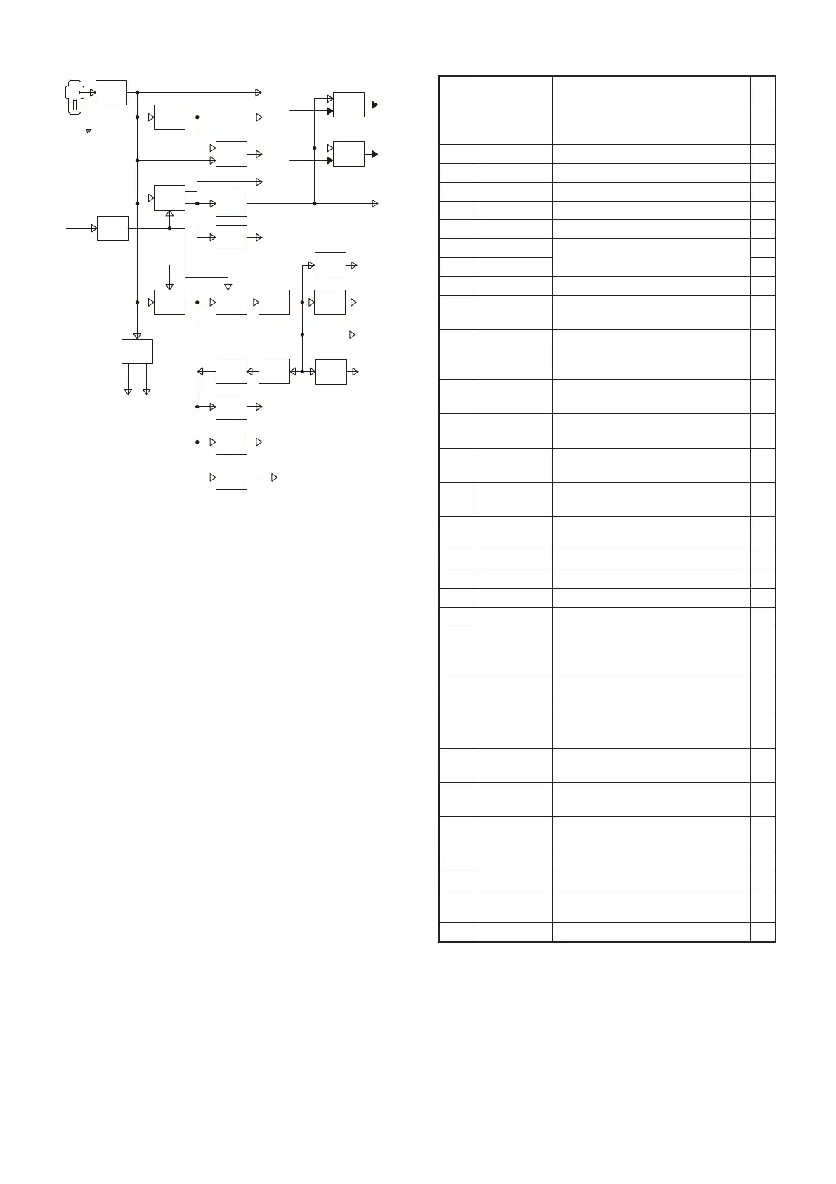
4-5 PORT ALLOCATIONS4-4 VOLTAGE DIAGRAM
 Loading...