Electrical Specifications
24 Datasheet
2.6.2 CMOS and Open Drain Signals
Legacy input signals such as A20M#, IGNNE#, INIT#, SMI#, and STPCLK# use CMOS
input buffers. All of the CMOS and Open Drain signals are required to be asserted/
deasserted for at least four BCLKs for the processor to recognize the proper signal
state. See Section 2.6.3 for the DC specifications. See Section 6.2 for additional timing
requirements for entering and leaving the low power states.
2.6.3 Processor DC Specifications
The processor DC specifications in this section are defined at the processor core (pads)
unless otherwise stated. All specifications apply to all frequencies and cache sizes
unless otherwise stated.
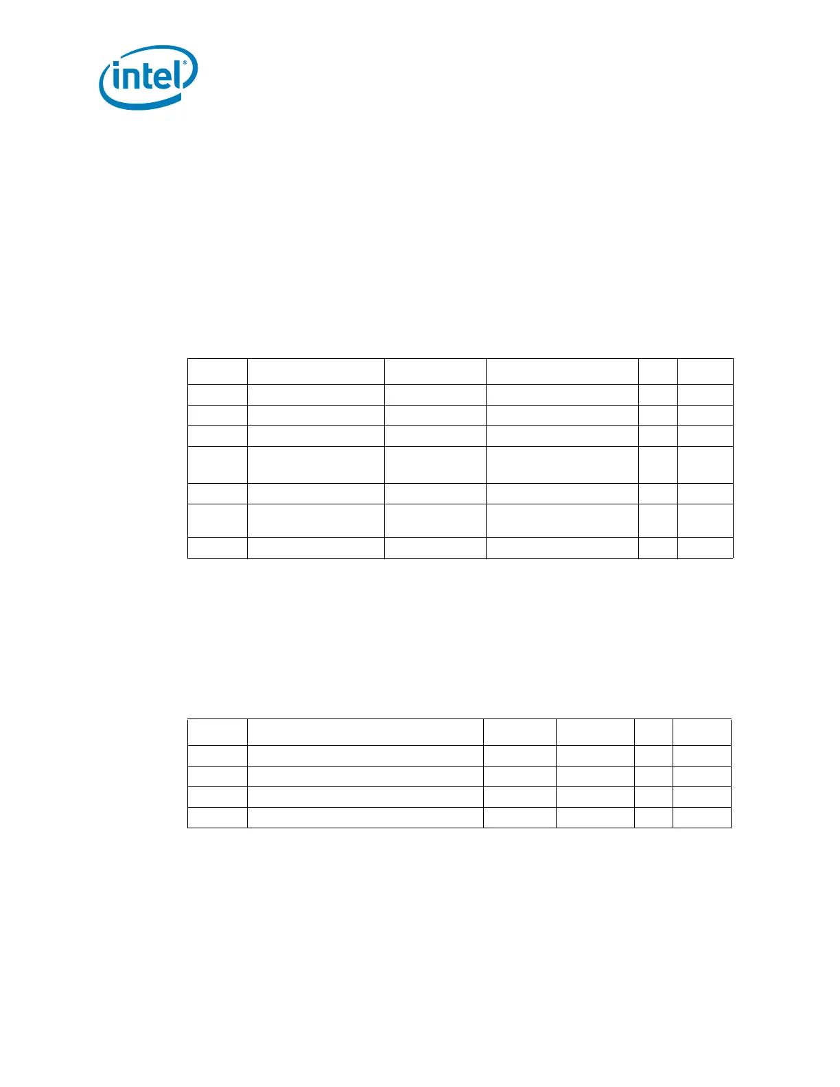
Table 10. GTL+ Signal Group DC Specifications
Symbol Parameter Min Max Unit Notes
1
NOTES:
1. Unless otherwise noted, all specifications in this table apply to all processor frequencies.
V
IL
Input Low Voltage -0.10 GTLREF – 0.10 V
2, 3
2. V
IL
is defined as the voltage range at a receiving agent that will be interpreted as a logical low
value.
3. The V
TT
referred to in these specifications is the instantaneous V
TT
.
V
IH
Input High Voltage GTLREF + 0.10 V
TT
+ 0.10 V
3, 4, 5
4. V
IH
is defined as the voltage range at a receiving agent that will be interpreted as a logical high
value.
5. V
IH
and V
OH
may experience excursions above V
TT
.
V
OH
Output High Voltage V
TT
– 0.10 V
TT
V
3, 5
I
OL
Output Low Current N/A
V
TT_MAX
/
[(R
TT_MIN
)+(2*R
ON_MIN
)]
A-
I
LI
Input Leakage Current N/A ± 200 µA
6
6. Leakage to V
SS
with land held at V
TT
.
I
LO
Output Leakage
Current
N/A ± 200 µA
7
7. Leakage to V
TT
with land held at 300 mV.
R
ON
Buffer On Resistance 10 13 Ω
Table 11. Open Drain and TAP Output Signal Group DC Specifications
Symbol Parameter Min Max Unit Notes
1
NOTES:
1. Unless otherwise noted, all specifications in this table apply to all processor frequencies.
V
OL
Output Low Voltage 0 0.20 V -
V
OH
Output High Voltage V
TT
– 0.05 V
TT
+ 0.05 V
2
2. V
OH
is determined by the value of the external pull-up resister to V
TT
.
I
OL
Output Low Current 16 50 mA
3
3. Measured at V
TT
* 0.2.
I
LO
Output Leakage Current N/A ± 200 µA
4
4. For Vin between 0 and V
OH
.
 Loading...


