Land Listing and Signal Descriptions
Datasheet 55
H30 BSEL1 Power/Other Output
J1 VTT_OUT_LEFT Power/Other Output
J2 FC3 Power/Other
J3 FC22 Power/Other
J4 VSS Power/Other
J5 REQ1# Source Synch Input/Output
J6 REQ4# Source Synch Input/Output
J7 VSS Power/Other
J8 VCC Power/Other
J9 VCC Power/Other
J10 VCC Power/Other
J11 VCC Power/Other
J12 VCC Power/Other
J13 VCC Power/Other
J14 VCC Power/Other
J15 VCC Power/Other
J16 FC31 Power/Other
J17 FC34 Power/Other
J18 VCC Power/Other
J19 VCC Power/Other
J20 VCC Power/Other
J21 VCC Power/Other
J22 VCC Power/Other
J23 VCC Power/Other
J24 VCC Power/Other
J25 VCC Power/Other
J26 VCC Power/Other
J27 VCC Power/Other
J28 VCC Power/Other
J29 VCC Power/Other
J30 VCC Power/Other
K1 LINT0 Asynch CMOS Input
K2 VSS Power/Other
K3 A20M# Asynch CMOS Input
K4 REQ0# Source Synch Input/Output
K5 VSS Power/Other
K6 REQ3# Source Synch Input/Output
K7 VSS Power/Other
K8 VCC Power/Other
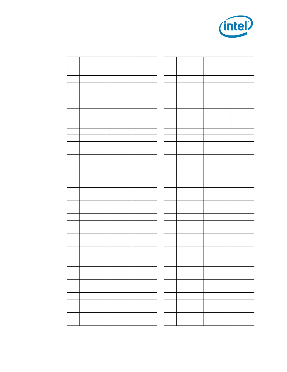
Table 24. Numerical Land
Assignment
Land
#
Land Name
Signal Buffer
Type
Direction
K23 VCC Power/Other
K24 VCC Power/Other
K25 VCC Power/Other
K26 VCC Power/Other
K27 VCC Power/Other
K28 VCC Power/Other
K29 VCC Power/Other
K30 VCC Power/Other
L1 LINT1 Asynch CMOS Input
L2 TESTHI13 Power/Other Input
L3 VSS Power/Other
L4 A06# Source Synch Input/Output
L5 A03# Source Synch Input/Output
L6 VSS Power/Other
L7 VSS Power/Other
L8 VCC Power/Other
L23 VSS Power/Other
L24 VSS Power/Other
L25 VSS Power/Other
L26 VSS Power/Other
L27 VSS Power/Other
L28 VSS Power/Other
L29 VSS Power/Other
L30 VSS Power/Other
M1 VSS Power/Other
M2 THERMTRIP# Asynch CMOS Output
M3 STPCLK# Asynch CMOS Input
M4 A07# Source Synch Input/Output
M5 A05# Source Synch Input/Output
M6 REQ2# Source Synch Input/Output
M7 VSS Power/Other
M8 VCC Power/Other
M23 VCC Power/Other
M24 VCC Power/Other
M25 VCC Power/Other
M26 VCC Power/Other
M27 VCC Power/Other
M28 VCC Power/Other
M29 VCC Power/Other
Table 24. Numerical Land
Assignment
Land
#
Land Name
Signal Buffer
Type
Direction
 Loading...


