Datasheet 25
Electrical Specifications
NOTE:
1. V
TT
supplies the PECI interface. PECI behavior does not affect V
TT
min/max specifications.
Refer to Table 4 for V
TT
specifications.
2. The leakage specification applies to powered devices on the PECI bus.
3. The input buffers use a Schmitt-triggered input design for improved noise immunity.
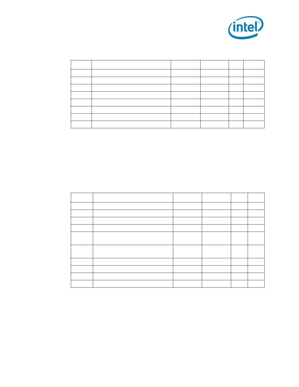
Table 12. CMOS Signal Group DC Specifications
Symbol Parameter Min Max Unit Notes
1
NOTES:
1. Unless otherwise noted, all specifications in this table apply to all processor frequencies.
V
IL
Input Low Voltage -0.10 V
TT
* 0.30 V
2, 3
2. V
IL
is defined as the voltage range at a receiving agent that will be interpreted as a logical low
value.
3. The V
TT
referred to in these specifications refers to instantaneous V
TT
.
V
IH
Input High Voltage V
TT
* 0.70 V
TT
+ 0.10 V
3, 4, 5
4. V
IH
is defined as the voltage range at a receiving agent that will be interpreted as a logical high
value.
5. V
IH
and V
OH
may experience excursions above V
TT
.
V
OL
Output Low Voltage -0.10 V
TT
* 0.10 V
3
V
OH
Output High Voltage 0.90 * V
TT
V
TT
+ 0.10 V
3, 5,6
6. All outputs are open drain.
I
OL
Output Low Current 1.70 4.70 mA
3, 7
7. I
OL
is measured at 0.10 * V
TT.
I
OH
is measured at 0.90 * V
TT.
I
OH
Output High Current 1.70 4.70 mA
3, 7
I
LI
Input Leakage Current N/A ± 100 µA
8
8. Leakage to V
SS
with land held at V
TT
.
I
LO
Output Leakage Current N/A ± 100 µA
9
9. Leakage to V
TT
with land held at 300 mV
Table 13. PECI DC Electrical Limits
Symbol Definition and Conditions Min Max Units Notes
V
in
Input Voltage Range -0.30 V
TT
V
V
hysteresis
Hysteresis 0.1 * V
TT
—V3
V
n
Negative-edge threshold voltage 0.275 * V
TT
0.500 * V
TT
V
V
p
Positive-edge threshold voltage 0.550 * V
TT
0.725 * V
TT
V
I
source
High level output source
(V
OH
= 0.75 * V
TT
)
-6.0 N/A mA
I
sink
Low level output sink
(V
OL
= 0.25 * V
TT
)
0.5 1.0 mA
I
leak+
High impedance state leakage to V
TT
N/A 50 µA 2
I
leak-
High impedance leakage to GND N/A 10 µA 2
C
bus
Bus capacitance —10pF
V
noise
Signal noise immunity above 300 MHz 0.1 * V
TT
—V
p-p

 Loading...