Electrical Specifications
28 Datasheet
2.7.4 BCLK[1:0] Specifications
.
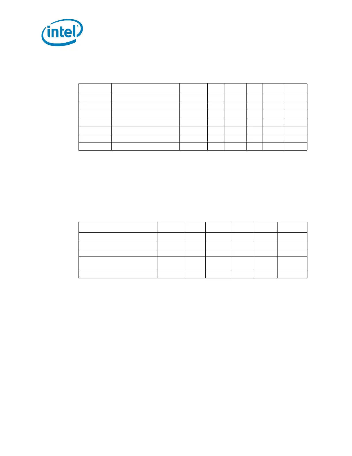
Table 17. Front Side Bus Differential BCLK Specifications
Symbol Parameter Min Typ Max Unit Figure Notes
1
NOTES:
1. Unless otherwise noted, all specifications in this table apply to all processor frequencies.
V
L
Input Low Voltage -0.30 N/A N/A V 3
2
2. "Steady state" voltage, not including overshoot or undershoot.
V
H
Input High Voltage N/A N/A 1.15 V 3
2
V
CROSS(abs)
Absolute Crossing Point 0.300 N/A 0.550 V 3, 4
3, 4, 5
3. Crossing voltage is defined as the instantaneous voltage value when the rising edge of BCLK0
equals the falling edge of BCLK1.
4. The crossing point must meet the absolute and relative crossing point specifications
simultaneously
5. V
Havg
is the statistical average of the V
H
measured by the oscilloscope.
ΔV
CROSS
Range of Crossing Points N/A N/A 0.140 V 3, 4 -
V
OS
Overshoot N/A N/A 1.4 V 3
6
6. Overshoot is defined as the absolute value of the maximum voltage. Undershoot is defined as
the absolute value of the minimum voltage.
V
US
Undershoot -0.300 N/A N/A V 3
6
V
SWING
Differential Output Swing 0.300 N/A N/A V 5
7
7. Measurement taken from differential waveform.
Table 18. FSB Differential Clock Specifications (1066 MHz FSB)
T# Parameter Min Nom Max Unit Figure Notes
1
NOTES:
1. Unless otherwise noted, all specifications in this table apply to all processor core frequencies
based on a 266 MHz BCLK[1:0].
BCLK[1:0] Frequency 265.307 — 266.746 MHz
2
2. Duty Cycle (High time/Period) must be between 40 and 60%.
T1: BCLK[1:0] Period 3.74963 — 3.76922 ns 3
3
3. The period specified here is the average period. A given period may vary from this specification
as governed by the period stability specification (T2). Min period specification is based on
-300 PPM deviation from a 3.75 ns period. Max period specification is based on the summation
of +300 PPM deviation from a 3.75 ns period and a +0.5% maximum variance due to spread
spectrum clocking.
T2: BCLK[1:0] Period Stability — — 150 ps 3
4
4. In this context, period stability is defined as the worst case timing difference between successive
crossover voltages. In other words, the largest absolute difference between adjacent clock
periods must be less than the period stability.
T5: BCLK[1:0] Rise and Fall Slew
Rate
2.5 — 8 V/nS 5
5
5. Measurement taken from differential waveform.
T6: Slew Rate Matching N/A N/A 20 %
6
6. Matching applies to rising edge rate for Clock and falling edge rate for Clock#. It is measured
using a ±75 mV window centered on the average cross point where Clock rising meets Clock#
falling. The median cross point is used to calculate the voltage thresholds the oscilloscope is to
use for the edge rate calculations.
 Loading...


