Chapter 5---Electronics
5-6 Model 250 Service Manual
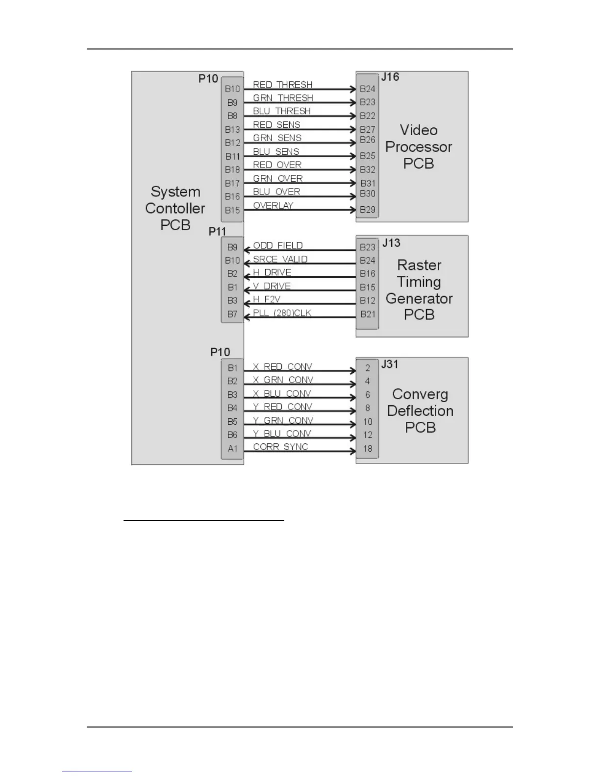
Figure 5-5
System Controller PCB I/O Diagram for other PCBs.
System Controller PCB - Inputs
/LV_OK - signal from the Low Voltage Power Supply; it tells the System
Controller PCB that all the non-standby supply voltages are working.
/HV_OK - signal from the High Voltage Power Supply; it tells the System
Controller PCB that all the high voltage supplies are working.
/LAMP_OK - signal from the Arc Lamp Power Supply.
/LAMP_LIT - signal from the Arc Lamp Power Supply; it tells the System
Controller PCB that the Arc Lamp is lit.
ODD_FIELD - Square wave signal from the Raster Timing Generator PCB, with
50% duty cycle that is low during odd fields of an Interlace signal. This signal is
high during noninterlaced signals.
 Loading...