9-6
Standard Bias Table Table 9-4, below, outlines some standard supply voltages and system
clocks which should be present under normal operation. These should
be checked as a first step to any troubleshooting procedure.
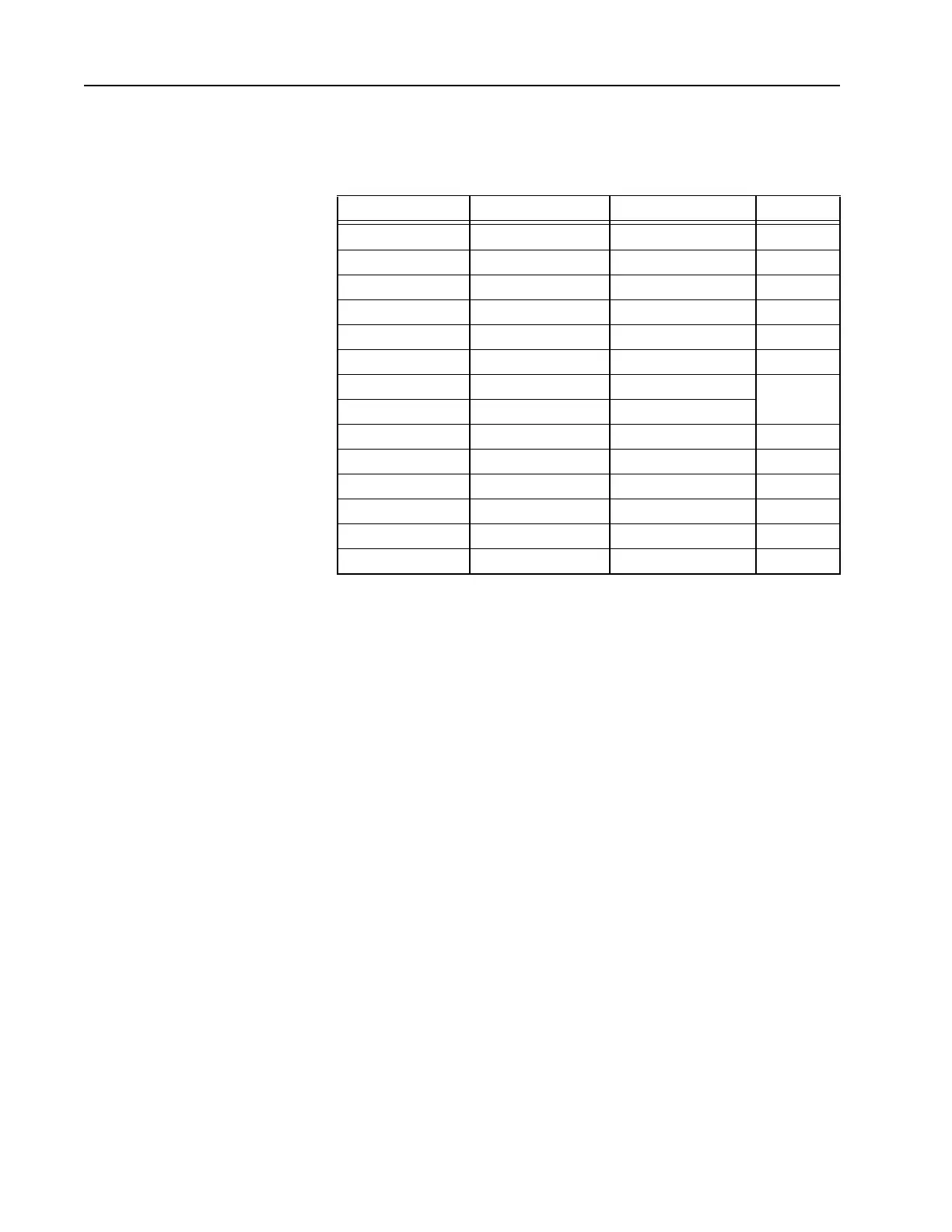
Table 9-4 Standard Operating Bias
Signal Name Nominal Value Tolerance Source
UNSW_B+ 7.5Vdc 6.0-9.0Vdc J101
SW_B+ 7.5Vdc 6.0-9.0Vdc Q106
+5V 5.0Vdc ±10% U709
+5VA 5.0Vdc ±10% U710
RESET 5.0Vdc +0.7, -1.0Vdc U702
POR* 5.0Vdc +0.7, -1.0Vdc U726
DSP_RST* 5.0Vdc +0.7, -1.0Vdc U701
ADSIC_RST* 5.0Vdc +0.7, -1.0Vdc
DCLK 33.0000MHz
a
a. This is number may vary due to the operating mode of the radio when
it is measured. The ADSIC contains a divider which may divide the
clock by a modulus of 2. Therefore the actual frequency measured
may be clock/2
n
. The most common frequency will be 16.5000MHz
nominal.
±500ppM U406
ODC 2.4MHz ±30ppM ABACUS
ECLK 1.8432MHz ±500ppM U701
IRQB* 8kHz
b
b. This 8kHz clock will be present only after the MCU has successfully pro-
grammed the ADSIC after power-up. This is a good indication that the
ADSIC is at least marginally operational.
±500ppM U406
+5V 5.0Vdc ±10% U202
RX_5V
c
c. Receive mode only.
5.0Vdc ±10% U106
 Loading...