Refer to the model specifications on ni.com/manuals for the real-time clock accuracy
specifications.
Digital Routing
The digital routing circuitry of the cRIO-904x manages the flow of data between the bus
interface and the acquisition and generation sub-systems when programming C Series modules
in Real-Time (NI-DAQmx) mode. The subsystems include analog input, analog output, digital
I/O, and counters. The digital routing circuitry uses FIFOs (if present) in each sub-system to
ensure efficient data movement.
Note When programming C Series modules in FPGA mode, the flow of data
between the modules and the bus interface is programmed using LabVIEW FPGA.
The digital routing circuitry also routes timing and control signals. The acquisition and
generation sub-systems use these signals to manage and synchronize acquisitions and
generations. These signals can come from the following sources:
• C Series modules programmed in Real-Time (NI-DAQmx) mode
• User input through the PFI terminals using parallel digital C Series modules or the
cRIO-904x PFI 0 terminal
• FPGA or DAQ ASIC using the cRIO trigger bus to share hardware triggers and signals
between the LabVIEW FPGA and DAQmx applications
Clock Routing
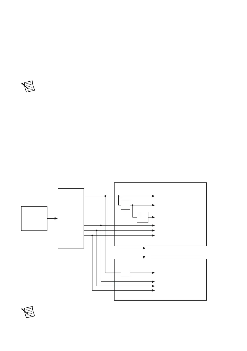
The following figure shows the clock routing circuitry of the cRIO-904x.
Figure 6. Clock Routing Circuitry of the cRIO-904x
Onboard
100 MHz
Oscillator
Clock
Generator
DAQ ASIC
RIO FPGA
cRIO Trigger Bus
80 MHz Timebase
20 MHz Timebase
100 kHz Timebase
13.1072 MHz Timebase
12.8 MHz Timebase
10 MHz Timebase
40 MHz Onboard Clock
÷200
13.1072 MHz Carrier Clock
12.8 MHz Carrier Clock
10 MHz Carrier Clock
÷2
÷4
Note When switching between programming modes, you may notice the terms
timebase and clock used interchangeably. This is due to the DAQ ASIC and the RIO
cRIO-904x User Manual | © National Instruments | 19
 Loading...