USB 2.0 Tuning Guide
PRELIMINARY INFORMATION
Jetson AGX Orin Series Tuning and Compliance Guide DA-11040-001_v0.7 | 4
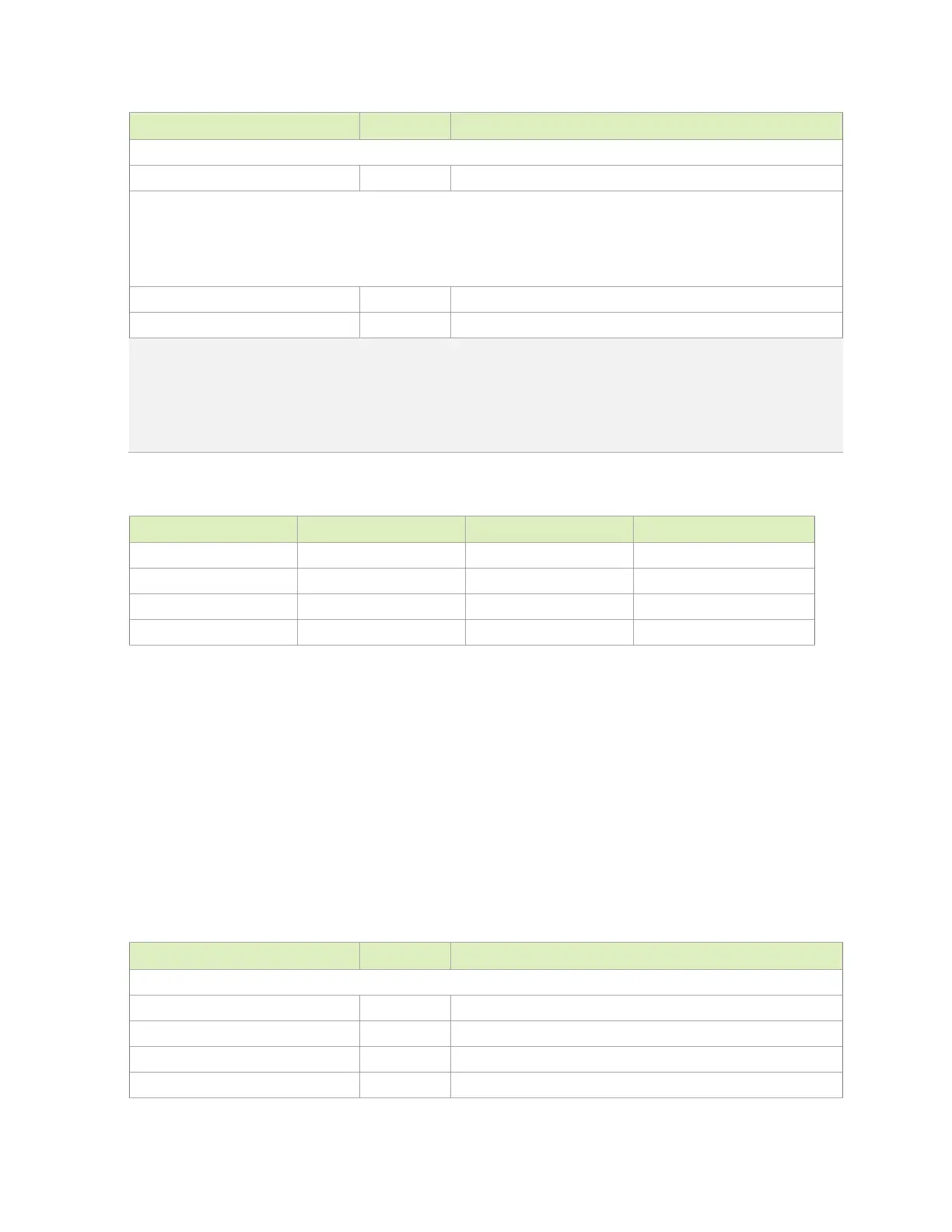
Register Name Bit Field Description
XUSB_PADCTL_USB2_BIAS_PAD_CTL_0_0 (Address 0x03520284)
HS_SQUELCH_LEVEL 2:0 HSSQUELCH (squelch level control for device RX testing)
XUSB_PADCTL_USB2_OTG_PAD0_CTL_3_0 (Address 0x03520094) for Port 0
XUSB_PADCTL_USB2_OTG_PAD1_CTL_3_0 (Address 0x035200D4) for Port 1
XUSB_PADCTL_USB2_OTG_PAD2_CTL_3_0 (Address 0x03520114) for Port 2
XUSB_PADCTL_USB2_OTG_PAD3_CTL_3_0 (Address 0x03520154) for Port 3
HS_RXEQ (See Note 3) 8:6 HS_RXEQ (device RX testing)
HS_TXEQ (See Note 3) 3:1 HS_TXEQ (device TX testing)
Notes:
1. HS_SLEW where 0’b000 = slowest and 0’b111 = fastest
2. HS_CURR_LEVEL where 0’b000000 = highest current level and 0’b111111 = lowest current level
3. If system has inner cable, consult with AE for recommendations and perform certificate and functional test
verification.
Table 3. TXEQ and RXEQ Pre-Emphasis
HS_TXEQ[2:0] AC Gain HS_RXEQ[2.0] SQ Level
00 +0 dB (default) 00 -0 dB (default)
01 +1.3 dB 01 -1.2 dB
10 +2.5 dB 10 -2.0 dB
11 +3.5 dB 11 -3.5 dB
Tuning Procedure and Registers
During production, each Orin SoC is calibrated based on the silicon process, the
corresponding USB drive strength (HS_CURR_LEVEL), HS termination (TERM_RANGE_ADJ),
and a 15K host pull-down (RPD_CTL). As a result, fuses are burnt on each chip.
Table 4 lists the breakdown for the USB_CALIB and USB_CALIB_EXT fuses. Reading from the
respective addresses will provide the default drive strength, HS termination, and 15K host
pull-down value.
Table 4. USB_CALIB and USB_CALIB_EXT Fuses
Register Name Bit Field Description
USB_CALIB fuse (Address 0x038201F0)
USB_CALIB 28:23 HS_CURR_LEVEL for USB Port 3
USB_CALIB 22:17 HS_CURR_LEVEL for USB Port 2
USB_CALIB 16:11 HS_CURR_LEVEL for USB Port 1
USB_CALIB 10:7 TERM_RANGE_ADJ for all USB ports

 Loading...


