PCIe Compliance Testing Reference
PRELIMINARY INFORMATION
Jetson AGX Orin Series Tuning and Compliance Guide DA-11040-001_v0.7 | 12
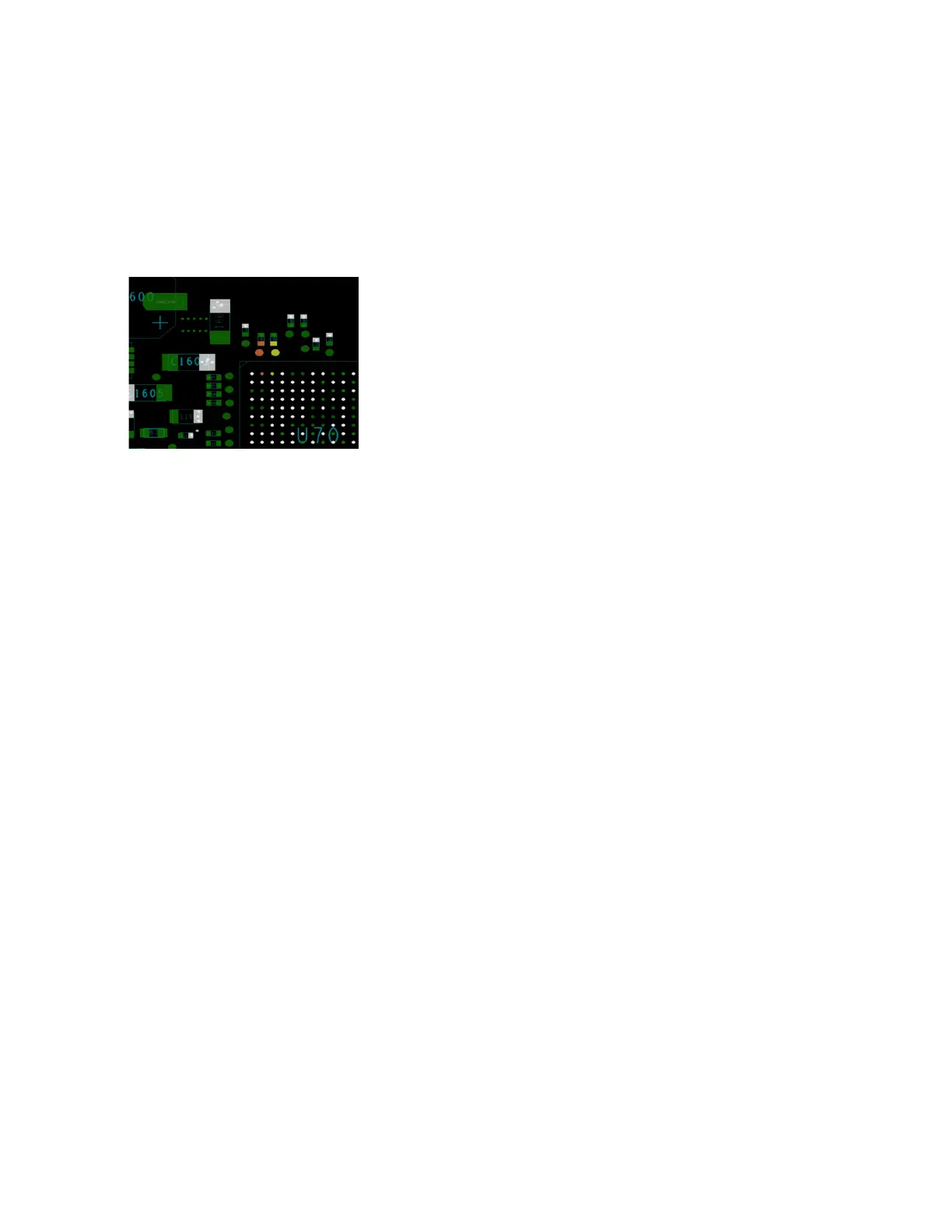
The following figure shows part of an Orin module reference design.
Note the following:
Device is removed to probe at the pins.
In the example, the Orin module sourced REFCLK. It shall be injected from external source.
Figure 1. Device Removed from PCB for Characterization Example
Mid-Bus Probing
Note that mid-bus probing is not used by NVIDIA for characterization. Customers may use
access points for probes that may be Rx or Tx coupling caps. Proper access to traces at
coupling caps with the least possible distortion is required. Mid-bus probing is a less intrusive
form of de-embedding. In turn, it requires S-PARAMS to be extracted from layout in between
the coupling cap and the “remaining trace.” Assume one taps into the Orin module Tx lane-n,
the coupling cap will be removed, and Orin module Tx lane-n will be probed at the coupling
cap (Orin module side). The S-PARAM extracted from layout must model the remaining trace
from the coupling cap to the device pins. A scope used in this DUT setup must be able to fold
in real-time filters for convoluting S-PARMS with real-time measurement to model the
“remaining trace” real time.
Oscilloscopes
An oscilloscope is used to measure and capture the signals for Tx characterization. It must
fulfill data signal bandwidth requirements. The oscilloscope bandwidth shall be above Nyquist
frequency. For Gen4 maximum bandwidth must be greater than or equal to 25 GHz and have a
minimum sample rate of 64 GS/s. For Gen3 it must be at least 13 GHz and 32 GS/s.
BERT
A Bit Error Rate Tester (BERT) may be used for Rx testing, for example, the Rx_LINK equalizer
test. The BERT must be capable of acting as a loop-back initiator to drive the DUT lanes
selected for test into loop-back mode with the BERT acting as a link partner using interactive
link training.

 Loading...