PCIe Compliance Testing Reference
PRELIMINARY INFORMATION
Jetson AGX Orin Series Tuning and Compliance Guide DA-11040-001_v0.7 | 21
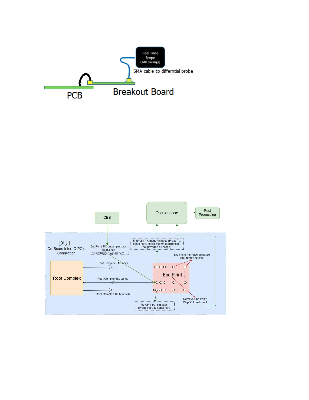
Figure 5. Breakout Board 50 Ω Differential Measurement Use
1. Connect breakout board #1 P+ / P- via SMA to differential probe CH1-CH3 (data).
2. Connect breakout board #3 P+ / P- via SMA to differential probe CH2-CH4 (clock).
3. Connect breakout board #2 P+ / P- via SMA to signal generator or CBB (see Figure 5).
When using CBB as pulse source, connect CBB J5/J85 to Rx lane-n P+ / P-. This will inject
the pulse used for pattern sequence change (preset) when the toggle push button is
pressed. Else, if a pulse generator is used in place of CBB then connect the pulse
generator to Rx lane-n.
Figure 6 shows a common clock (CC) configuration.
Figure 6. Orin Probing Diagram with PCIe Device Removed

 Loading...